25 Linearity by Synthesis: An Intrinsically Linear AlGaN/GaN-on-Si Transistor with OIP3/(F-1)PDC of 10.1 at 30 GHz
Category
Published on
Abstract
Introduction: In today’s radio-frequency (RF) systems, linearity of amplifiers is a key concern due to presence of significant numbers of in-band interferers in the crowded spectrum. GaN high electron mobility transistors (HEMTs) can provide low noise front-end amplifiers, but state-of-the-art GaN HEMTs still possess non-linearity exhibited by a transconductance, gm, roll-off from its peak due to the dynamic source access resistance and other factors [1]. The dynamic range figure-of-merit (DRFOM) for low noise amplifiers (LNAs) [2], OIP3/(F-1)PDC, where OIP3 is the output 3rd-order intercept point (OIP3), PDC is the DC power, and F is the noise factor, is still limited to ~1.7 in mm-wave GaN transistors [3]. Joglekar et al. attempted to increase linearity by using different Fin widths resulted in flat gm of ~2 V [1]; linearity figures of merit were not properly assessed. Here, we demonstrate a novel method to synthesize gm plateau over a 6 V gate overdrive and a record DRFOM of 10.1 in GaN HEMTs at 30 GHz.
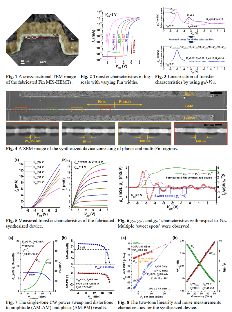
Experiment and Device Design: The metal-insulator-semiconductor (MIS) structure incorporates a planar FET in parallel with a set of fin FETs. A commercial Al0.23Ga0.77N/GaN-on-Si wafer was used without additional epitaxial layer growth. An alloyed Ti/Al-based Ohmic contact was used and Fin structures were formed by e-beam lithography and dry etching. Fin widths (WFin) were varied from 50 nm to 200 nm, and fin length (LFin), gap between Fins (Wgap), and mesa width (WM) were fixed at 150 nm, 200 nm, and 20 μm, respectively. A 6 nm-thick Al2O3 was deposited by atomic layer deposition (ALD), and a Ti/Au gate metal was evaporated. After opening ohmic windows, Ti/Au pads and Si3N4 passivation layers were deposited. The gate-to-source (LGS), gate-to-drain distances (LGD), and a gate length (LG) were 0.5 μm, 1.35 μm, and 90 nm, respectively. Figure 1 shows the cross-sectional transmission electron microscopy (TEM) image of the fabricated Fin metal-insulator-semiconductor (MIS) structure.
In Fin MIS-HEMTs, as shown in Figure 2, threshold voltages (VT) shift in positive direction with decreasing WFin, because of the tri-gate structure [4]. For a device composed of a planar and several Fin channels, termed a synthesized device, ID can be expressed as: ID,total (VGS) = a0ID,0(VGS - VT,0) + a1ID,1(VGS-VT,1) + ⋯ + ak ID,k (VGS - Vt,k), where ak is the weight of kth channels for a family of Fins with a width, WFin,k, and a threshold voltage, VT,k. k=0 represents the planar device characteristics. We chose 4 different WFin of 160, 100, 80, and 50 nm to linearize the transfer characteristic of the planar device. As shown in Figure 3, we exploited gm' for the selected WFin and computed ak to obtain a wide zero gm' window for VGS from -4 V to 2 V. Figure 4 shows a scanning electron microscopy (SEM) image of the fabricated synthesized device. Figure 5(a) and (b) are the linearized transfer characteristic showing a gm plateau of ~6 V and the output characteristics, respectively. Figure 6 shows measured gm and its derivatives with multiple gm" sweet spots.
LNA Performance at 30 GHz The planar-Fin synthesis design was adapted to another device with 8-fingers, 90 nm T-gates, a shorter LGS of 250 nm, and LGD of 350 nm on the same die for mm-wave LNAs. The device was biased at VDS=3 V and ID=63 mA in the following single-tone continuous wave (CW) power sweep and two-tone linearity measurements at 30 GHz at Maury Microwave with the source and load impedances matched to Γin* and 0.17∠140°, respectively. As can be seen in Figure 7(a), the single-tone CW power sweep measurement shows maximum output power (Pout), linear gain, and peak power added efficiency (PAE) of 19.6 dBm, 7.52 dB, and 32.35%, respectively. Figure 7(b) shows the measured distortions to amplitude (AM-AM (|S21|)), and to phase (AM-PM (∡S21)). The output 1-dB gain compression point (P1dB) was as high as 17.8 dBm. The AM-PM distortion was only 0.3 degree at P1dB. As shown in Figure 8(a), the input 3rd-order intercept point (IIP3) of 23.5 dBm and OIP3 of 31 dBm were extrapolated at a PDC of 189 mW. The ratio of carrier-to-IM3 (C/IM3) was above 45 dBc at Pin per tone of 0 dBm. On-wafer noise measurement was also carried out with frequencies from 8 to 50 GHz. The minimum noise figure (NFmin) and the associated gain (Ga) are shown in Figure 8(b), and the NFmin was 2.2 dB at 30 GHz, resulting in the LNA FOM of 10.1. To the best of our knowledge, this value is the record in GaN-based devices.
Conclusion The concept of an intrinsically synthesizable linear device is demonstrated. It was implemented by changing only the device layout; additional performance gains can be attained by further materials engineering.
Credits
The authors acknowledge the support of Renjie Chen for TEM, nano3 and Center for Integrated Nanotechnologies (CINT). This work was supported in part by an NSF-ECCS award #1711030.
References
- S. Joglekar et al., IEDM Tech. Dig., p. 613, (2017).
- V. Aparin et al., IEEE TMTT, p. 571, (2005).
- M. Micovic et al., CSICS Tech. Dig., p.1, (2016).
- J. Ma et al., IEEE TED, vol. 66, p. 4068, (2019).
Cite this work
Researchers should cite this work as follows:
Time
Location
DRC 2020 Virtual Conference