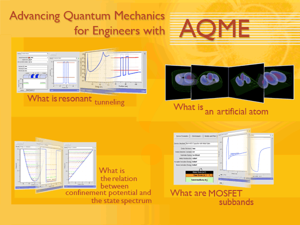
AQME: Advancing Quantum Mechanics for Engineers
Real World Applications
Real World Applications


Available resources:
 Right panel – Potential diagram for inversion of p-type semiconductor. In this first notation ?ij refers to the j-th subband from either the ?2-band (i=1) or ?4-band (i=2). Left panel – Constant-energy surfaces for the conduction-band of silicon showing six conduction-band valleys in the direction of momentum space. The band minima, corresponding to the centers of the ellipsoids, are 85% of the way to the Brillouin-zone boundaries. The long axis of an ellipsoid corresponds to the longitudinal effective mass of the electrons in silicon, while the short axes correspond to the transverse effective mass . For orientation of the surface, the ?2-band has the longitudinal mass (ml) perpendicular to the semiconductor interface and the ?4-band has the transverse mass (mt) perpendicular to the interface. Since larger mass leads to smaller kinetic term in the Schrodinger equation, the unprimed lader of subbands (as is usually called), corresponding to the ?2-band, has the lowest ground state energy. The degeneracy of the unprimed ladder of subbands for orientation of the surface is 2. For the same reason, the ground state of the primed ladder of subbands corresponding to the ?4-band is higher that the lowest subband of the unprimed ladder of subbands, The degeneracy of the primed ladder of subbands for (100) orientation of the interface is 4.
1-D Heterostructure Tool AQME
The 1-D Heterostructure Tool AQME simulates confined states in 1-D heterostructures by calculating charge self-consistently in the confined states, based on a quantum mechanical description of the one dimensional device. The greater interest in HEMT devices is motivated by the limits that will be reached with scaling of conventional transistors. The 1D Heterostructure Tool in that respect is a very valuable tool for the design of HEMT devices as one can determine, for example, the position and the magnitude of the delta-doped layer, the thickness of the barrier and the spacer layer for which one maximizes the amount of free carriers in the channel which, in turn, leads to larger drive current. This is clearly illustrated in the examples below.


- Uniform versus delta doping in 1D heterostructures: an Exercise
- Parallel Conduction Channel: an Exercise for 1D Heterostructure Lab
The most commonly used semiconductor devices for applications in the GHz range now are GaAs based MESFETs, HEMTs and HBTs. Although MESFETs are the cheapest devices because they can be realized with bulk material, i.e. without epitaxially grown layers, HEMTs and HBTs are promising devices for the near future. The advantage of HEMTs and HBTs is a factor of 2 to 3 higher power density compared to MESFETs which leads to significantly smaller chip size.
HEMTs are field effect transistors where the current flow between two ohmic contacts, Source and Drain, and it is controlled by a third contact, the Gate. Most often the Gate is a Schottky contact. In contrast to ion implanted MESFETs, HEMTs are based on epitaxially grown layers with different band gaps Eg. A schematic cross section of a HEMT is shown below.
 Schematic cross section of a High Electron Mobility Transistor (HEMT).
 If two semiconductors with different band gap energies are joined together, the difference is divided up into a band gap offset in the valence band ?EV and a band gap offset in the conduction band ?EC. One of the most common assumptions made for the AlGaAs/InGaAs material system is 40% valence band offset and 60% conduction band offset. This is only valid for Al contents below about 45%. For higher Al contents the bandgap of AlGaAs changes from direct to indirect. In the figure below such an AlGaAs/InGaAs HEMT with a delta doped upper barrier layer is shown. The conduction band energy under the gate along the cutting line A-A’ is shown to the right.
Resonant Tunneling Diode Lab in AQME


Put a potential barrier in the path of electrons, and it will block their flow; but, if the barrier is thin enough, electrons can tunnel right through due to quantum mechanical effects. It is even more surprising that, if two or more thin barriers are placed closely together, electrons will bounce between the barriers, and, at certain resonant energies, flow right through the barriers as if there were none. Run the Resonant Tunneling Diode Lab in AQME, which lets you control the number of barriers and their material properties, and then simulate current as a function of bias. Devices exhibit a surprising negative differential resistance, even at room temperature. This tool can be run online in your web browser as an active demo.


Available resources:
Quantum Dot Lab in AQME
Individual quantum dots can be created from two-dimensional electron or hole gases present in remotely doped quantum wells or semiconductor heterostructures. The sample surface is coated with a thin layer of resist. A lateral pattern is then defined in the resist by electron beam lithography. This pattern can then be transferred to the electron or hole gas by etching, or by depositing metal electrodes (lift-off process) that allow the application of external voltages between the electron gas and the electrodes. Such quantum dots are mainly of interest for experiments and applications involving electron or hole transport, i.e., an electrical current. The energy spectrum of a quantum dot can be engineered by controlling the geometrical size, the shape, and the strength of the confinement potential. Also, in contrast to atoms, it is relatively easy to connect quantum dots by tunnel barriers to conducting leads, which allows the application of the techniques of tunneling spectroscopy for their investigation. Confinement in quantum dots can also arise from electrostatic potentials (generated by external electrodes, doping, strain, or impurities).
 Quantum Dot Lab in AQME computes the eigenstates of a particle in a box of various shapes, including domes and pyramids.
Available resources:
- Quantum Dots is a nano 101, introductory lecture that starts from particle-wave duality and explores the concepts of quantum dots.
- Introduction to Quantum Dot Lab (by Lee, Ryu, Klimeck)
- Quantum Dot Lab Learning Module: An Introduction (by Fodor, Guo)
- Quantum Dot Spectra, Absorption, and State Symmetry: an Exercise