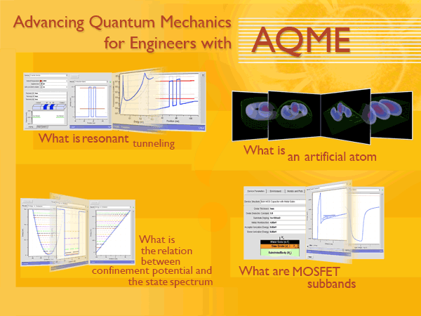
AQME: Advancing Quantum Mechanics for Engineers
Energy Bands and Effective Masses
Energy Bands and Effective Masses
Periodic Potential Lab in AQME

 The Periodic Potential Lab in AQME solves the time-independent Schrödinger Equation in a 1-D spatial potential variation. Rectangular, triangular, parabolic (harmonic), and Coulomb potential confinements can be considered. The user can determine energetic and spatial details of the potential profiles, compute the allowed and forbidden bands, plot the bands in a compact and an expanded zone, and compare the results against a simple effective mass parabolic band. Transmission is also calculated. This lab also allows the students to become familiar with the reduced zone and expanded zone representation of the dispersion relation (E-k relation for carriers).
Available resources:
Periodic Potentials and Bandstructure: an Exercise
Band Structure Lab in AQME

 Band structure of Si (left panel) and GaAs (right panel).
In solid-state physics, the electronic band structure (or simply band structure) of a solid describes ranges of energy that an electron is “forbidden” or “allowed” to have. It is due to the diffraction of the quantum mechanical electron waves in the periodic crystal lattice. The band structure of a material determines several characteristics, in particular, its electronic and optical properties. The Band Structure Lab in AQME enables the study of bulk dispersion relationships of Si, GaAs, InAs. Plotting the full dispersion relation of different materials, students first get familiar with a band structure of a direct band gap (GaAs, InAs), as well as indirect band gap semiconductors (Si). For the case of multiple conduction band valleys, students must first determine the Miller indices of one of the equivalent valleys, then, from that information they can deduce how many equivalent conduction bands are in Si and Ge, for example. In advanced applications, the users can apply tensile and compressive strain and observe the variation in the band structure, band gaps, and effective masses. Advanced users can also study band structure effects in ultra-scaled (thin body) quantum wells, and nanowires of different cross sections. Band Structure Lab uses the sp3s*d5 tight-binding method to compute E(k) for bulk, planar, and nanowire semiconductors.
Available resource:
Bulk Band Structure: a Simulation Exercise
 The figure on the left illustrates the first Brillouin zone of FCC lattice that corresponds to the first Brillouin zone for all diamond and Zinc-blende materials (C, Si, Ge, GaAs, InAs, CdTe, etc.). There are 8 hexagonal faces (normal to 111) and 6 square faces (normal to 100). The sides of each hexagon and each square are equal.
Supplemental Information: Specification of High-Symmetry Points
| Symbol | Description |
| G | Center of the Brillouin zone |
| Simple Cube | |
| M | Center of an edge |
| R | Corner point |
| X | Center of a face |
| Face-Centered Cubic | |
| K | Middle of an edge joining two hexagonal faces |
| L | Center of a hexagonal face |
| U | Middle of an edge joining a hexagonal and a square face |
| W | Corner point |
| X | Center of a square face |
| Body-Centered Cubic | |
| H | Corner point joining four edges |
| N | Center of a face |
| P | Corner point joining three edges |
| Hexagonal | |
| A | Center of a hexagonal face |
| H | Corner point |
| K | Middle of an edge joining two rectangular faces |
| L | Middle of an edge joining a hexagonal and a rectangular face |
| M | Center of a rectangular face |