IWCN 2021: Interfacial Trap Effects in InAs Gate-all-around Nanowire Tunnel Field- Effect Transistors: First-Principles-Based Approach
Category
Published on
Abstract
III-V materials have been actively adopted for the channel material to improve on-current of tunnel field-effect transistors (TFETs). But, one of the issues in practical III-V channel TFETs is the possible presence of interfacial traps between III-V channel and dielectric oxide [1]. A recent first-principles study reported that the dangling bond and anti-site traps can induce the bandgap states which critically affect the TFET performance [2]. However, the effects of these traps using full quantum transport simulation has not yet been investigated. To correctly understand the trap effects and provide practical guidelines for better TFET performance, it is essential to rigorously capture the impact of trapped charges and trap-assisted tunneling (TAT). In this work, we investigated the effects of the traps, Arsenic dangling bond (AsDB) and Arsenic anti-site (AsIn) traps, in InAs gate-all-around nanowire TFETs, using the trap Hamiltonian obtained from the first-principles calculations. The transport properties were treated by nonequilibrium Green’s function including the phonon scattering with self-consistent Born approximation. We have focused on the effects of the gate length (LG) and the trap position (xT).
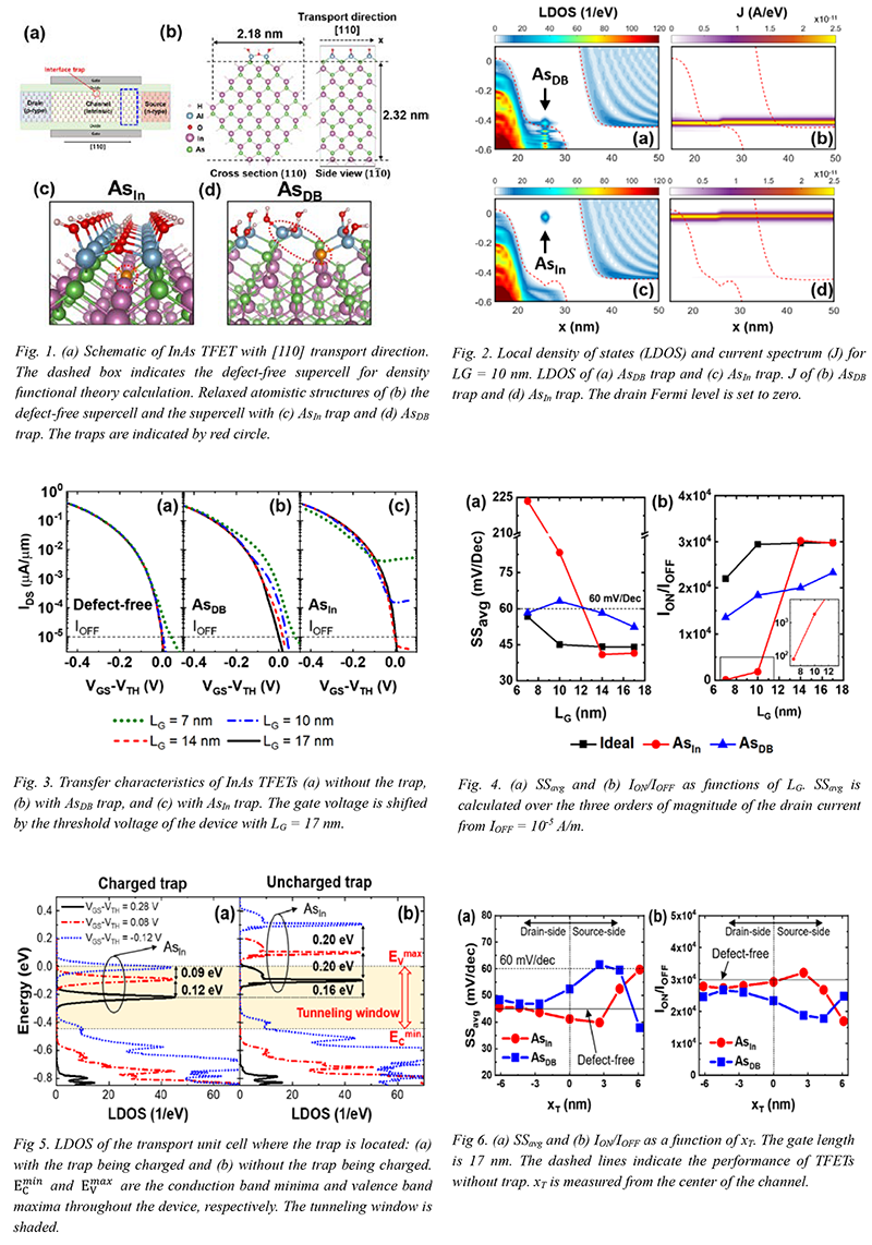
The schematic of the simulated device are shown in Fig. 1. Local density of state and current spectrums are shown in Fig. 2, where the AsDB trap is located above the valence band edge and the AsIn trap is at the midgap. Fig. 3 shows the transfer characteristics for LG = 7, 10, 14, and 17 nm. The traps mainly affect the subthreshold properties, and the impact becomes more significant as LG decreases. The average SS (SSavg) and ION/IOFF are depicted in Fig. 4 which reveals that the AsIn trap is the most detrimental trap for deep LG scaling. Fig. 5 shows that the degradation by the AsIn trap is caused by the trap charges (hole) which effectively block the gate electric field so that the TAT leakage current continues to take place. The effect of xT is shown in Fig. 6 which shows that even a single trap can have significant effects on the reliability and the traps located near source-side are more responsible than the traps near drain-side.
Credits
This work was supported by Samsung Research funding and the Incubation Center of Samsung Electronics under project number SRFC-TA1703-10
Sponsored by
References
- M. R. Tripathy et al, IEEE Trans. Electron Devices, 67, 1285 (2020)
- G. Greene-Diniz et al, J. Appl. Phys., 121, 075703 (2017)
Cite this work
Researchers should cite this work as follows: