Engineered Defects in Wide Band-gap Semiconductors for Single-spin Sensing and Computation
Category
Published on
Abstract
While generally considered undesirable in traditional electronic devices, semiconductor defects can confine isolated electronic spins and act as nanoscale, single-spin memory registers. Alongside research efforts focusing on nitrogen-vacancy centers in diamond, an alternative approach seeks to identify and control new spin systems in new materials, a strategy that could ultimately lead to “designer” spins with tailored properties for future quantum photonics and nanoscale sensing applications. Using infrared light at near-telecom wavelengths, I will show that spin states in silicon carbide exhibit long quantum coherence times that persist up to room temperature. I will also discuss new strategies for generating coherent spin interactions at the nanoscale using defects in inequivalent lattice sites (Fig. 1), as well as resonant electric and strain fields. Together with the availability of industrial scale crystal growth and advanced microfabrication, wide-gap semiconductors are promising platforms for room-temperature quantum technologies that merge spin degrees of freedom with electronics and photonics.
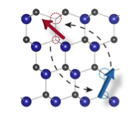
Fig. 1. Interacting spin states based on inequivalent defects in SiC
Sponsored by
Cite this work
Researchers should cite this work as follows:
Time
Location
Birck Technology Center, Room 1001, Purdue University, West Lafayette, IN