IWCN 2021: Ab initio Quantum Transport Simulation of Lateral Heterostructures Based on 2D Materials: Assessment of the Coupling Hamiltonians
Category
Published on
Abstract
Lateral heterostructures based on lattice-matched 2D materials are a promising option to design efficient electron devices such as MOSFETs [1], tunnel-FETs [2] and energy-filtering FETs [3]. In order to rigorously describe the transport through such heterostructures, an ab-initio approach based on density-functional theory (DFT) is almost unavoidable due to the lack of physical characterization of the interfaces. However, due to the computational cost of including the DFT Hamiltonian describing the whole interface region in transport calculations, the matrix describing the coupling between the two materials is often approximated as the one of a single material. Here, we focus on a simple lateral heterostructure based on bi-layer/mono-layer PtSe2 and compare the use of the coupling Hamiltonian matrix of the mono-layer PtSe2 with the one extracted from the DFT simulation of the whole bi- layer/mono-layer PtSe2 interface. To perform our self-consistent quantum transport calculations, we used the NEGF method and a reduced basis composed of unit-cell restricted Bloch functions [4]. To compute the coupling Hamiltonian between the bi- and the mono-layer PtSe2, we first performed a DFT simulation of the heterostructure sketched in Fig.1, where the dangling bonds at the interfaces are passivated by H atoms and all atomic positions have been relaxed. Hence, the plane-wave DFT Hamiltonian was transformed in the hybrid space having real-space along the x-axis and plane waves in the orthogonal directions, then, the block-matrix Hamiltonians representing the coupling between the two materials were extracted by selecting specific elements of the whole Hamiltonian and further reduced in the Bloch function basis.
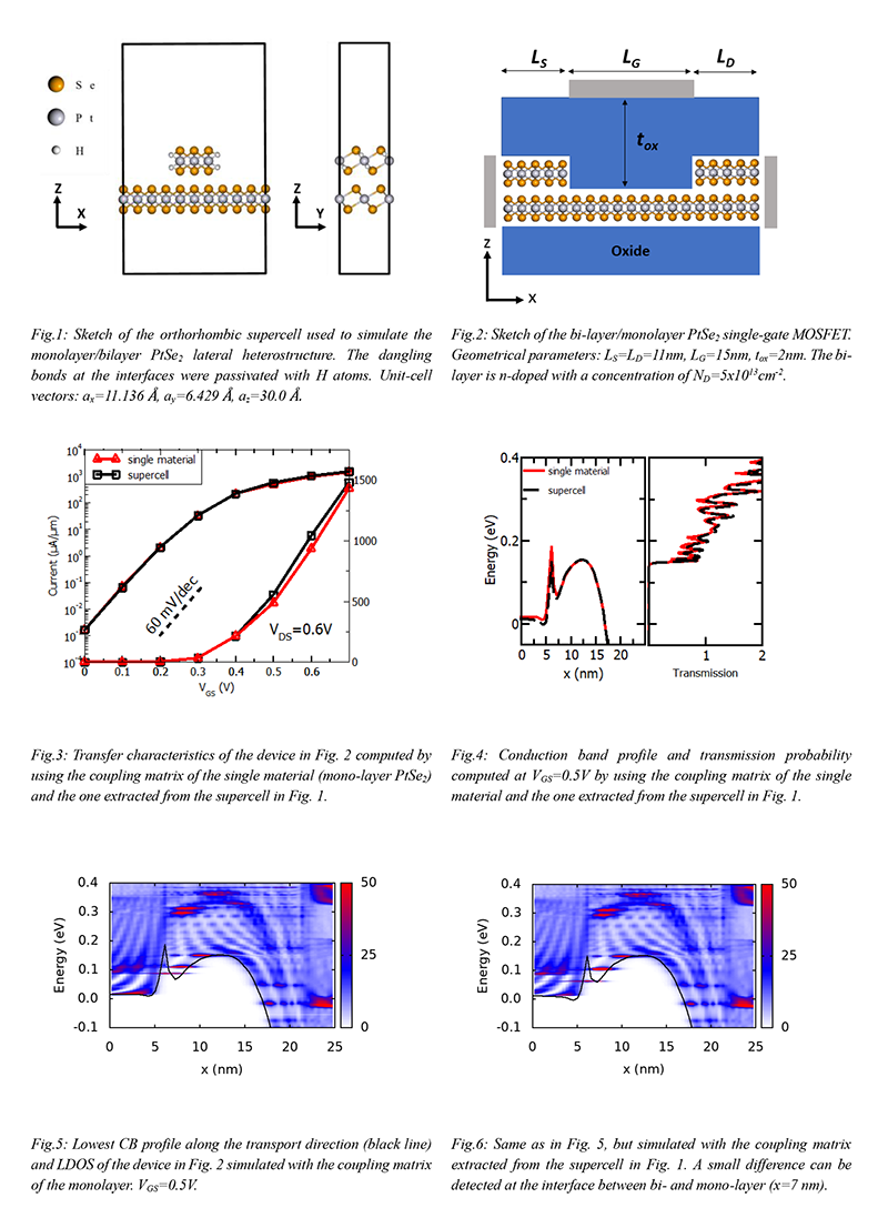
Fig. 3 shows the transfer characteristics of the bi-layer/mono-layer PtSe2 MOSFET in Fig.2 computed with either the coupling Hamiltonian of the mono-layer or the one extracted from the supercell in Fig 1. An appreciable difference is found at high VGS values. Fig. 4 shows the comparison between the lowest conduction band (LCB) profile and the transmission probability of such a device computed with the two types of coupling matrix. The second method provides a more efficient coupling between the two materials and consequently a larger transmission. A similar analysis can be extracted from Figs. 5-6 showing the local density of states at high VGS.
Bio
Sponsored by
References
- [1] G. Iannaccone et al. Nat. Nanotechnol. 13, 183–191 (2018).
- J. Choukroun et al., Nanotechnology 30, 025201 (2018).
- E. Marin et al., ACS Nano, 14, 2, 1982-1989 (2020).
- M. G. Pala et al., Phys. Rev. B., 102, 045410 (2020).
Cite this work
Researchers should cite this work as follows: