IWCN 2021: Multiscale Modeling and Simulation of Advanced Photovoltaic Devices
Category
Published on
Abstract
The introduction of new materials, device concepts and nanotechnology-based solutions to achieve high efficiency and low cost in photovoltaic (PV) devices requires modeling and simulation well beyond the current state of the art. New materials and heterojunction interfaces require atomistic approaches to understand their electronic and optical properties. Current commercial photovoltaic device simulators based on classical drift and diffusion models are limited in terms of describing nonequilibrium physics in critical regions of conventional devices and in far from equilibrium carrier dynamics in advanced concept devices (e.g. multi-exciton and hot carrier solar cells). At the same time, the characteristic time scales to describe the physics of solar cells span many orders of magnitude, ranging from femtoseconds for carrier dynamics to milliseconds for characteristic lifetimes. Length scales vary similarly from nanometers at interfaces to centimeters for the solar cell apertures. Therefore, accurate modeling of the microscopic physics in critical regions of the device have to be coupled with less accurate, but more macroscopic models, over long time periods and large simulation domain sizes.
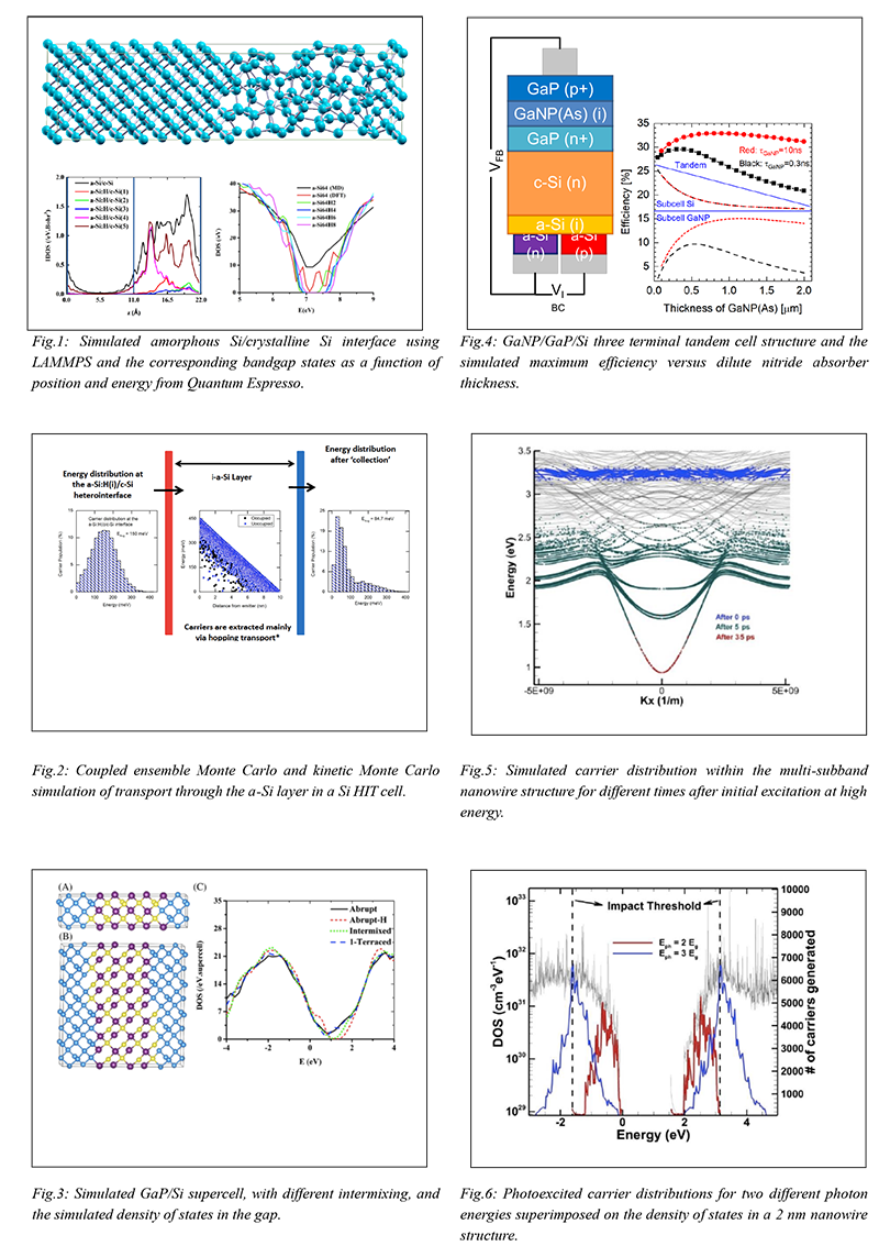
In this presentation, we discuss multiscale approaches used by our group in the modeling and simulation of several PV technologies, combining first principles modeling and transport simulation with commercial simulation tools. We first discuss crystalline Si/amorphous Si heterojunction devices, which have the highest reported efficiencies (>26%) for any Si technology [1], and the role of transport through the amorphous Si layers (Figures 1 and 2). We then discuss III-V on Si multi-junction solar cells for taking Si technology beyond its current single gap thermodynamic limits, and modeling of the heteropolar GaP/Si interface, and dilute nitrides for lattice matching and their optical and transport properties, and finally the impact on the expected two junction efficiency (Figures 3 and 4). The talk then concludes with a discussion of atomistic modeling of ultrafast carrier dynamics in nanowire arrays for application in multi-exciton generation and hot carrier solar cells [2] (Figures 5 and 6).
Bio
Yongjie Zou , Reza Vatan Meidanshahi , Raghuraj Hathwar , and Stephen Goodnick 1 School of Electrical Computer and Energy Engineering, Arizona State University, Tempe, Arizona 85287 USA goodnick@asu.edu
Sponsored by
References
- K. Yoshikawa et al., Nat. Energy, 4,17032 (2017)
- R. Hathwar et al., Topical Review in Journal of Physics D: Applied Physics 52, 093001 (2019).
Cite this work
Researchers should cite this work as follows: