FDNS21: Conversion of Metal Oxide Films to 2D Metal Chalcogenide Films

FDNS21: Conversion of Metal Oxide Films to 2D Metal Chalcogenide Films


-
 1. Conversion of Metal Oxides to …
0
00:00/00:00
1. Conversion of Metal Oxides to …
0
00:00/00:00 -
 2. Outline
37.337337337337338
00:00/00:00
2. Outline
37.337337337337338
00:00/00:00 -
 3. Outline
76.676676676676678
00:00/00:00
3. Outline
76.676676676676678
00:00/00:00 -
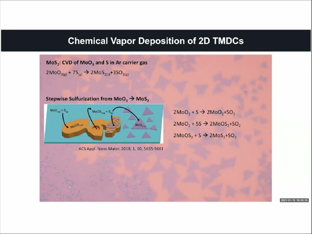 4. Chemical Vapor Deposition of 2…
85.318651985318652
00:00/00:00
4. Chemical Vapor Deposition of 2…
85.318651985318652
00:00/00:00 -
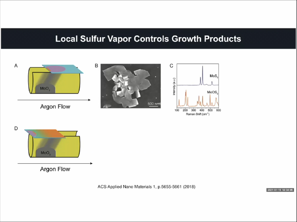
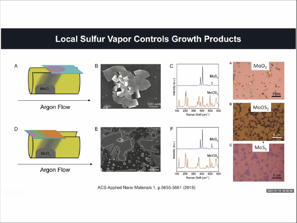 5. Local Sulfur Vapor Controls Gr…
153.01968635301969
00:00/00:00
5. Local Sulfur Vapor Controls Gr…
153.01968635301969
00:00/00:00 -
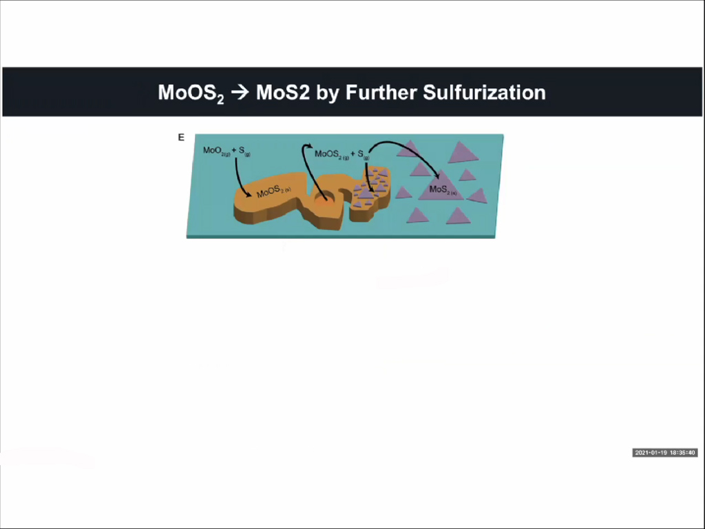
 6. MoOS2 -> MoS2 by Further Sulfu…
249.28261594928262
00:00/00:00
6. MoOS2 -> MoS2 by Further Sulfu…
249.28261594928262
00:00/00:00 -
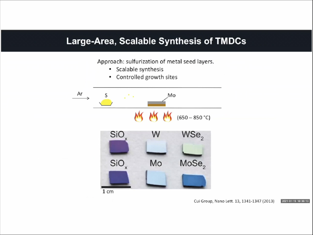 7. Large-Area, Scalable Synthesis…
287.88788788788787
00:00/00:00
7. Large-Area, Scalable Synthesis…
287.88788788788787
00:00/00:00 -
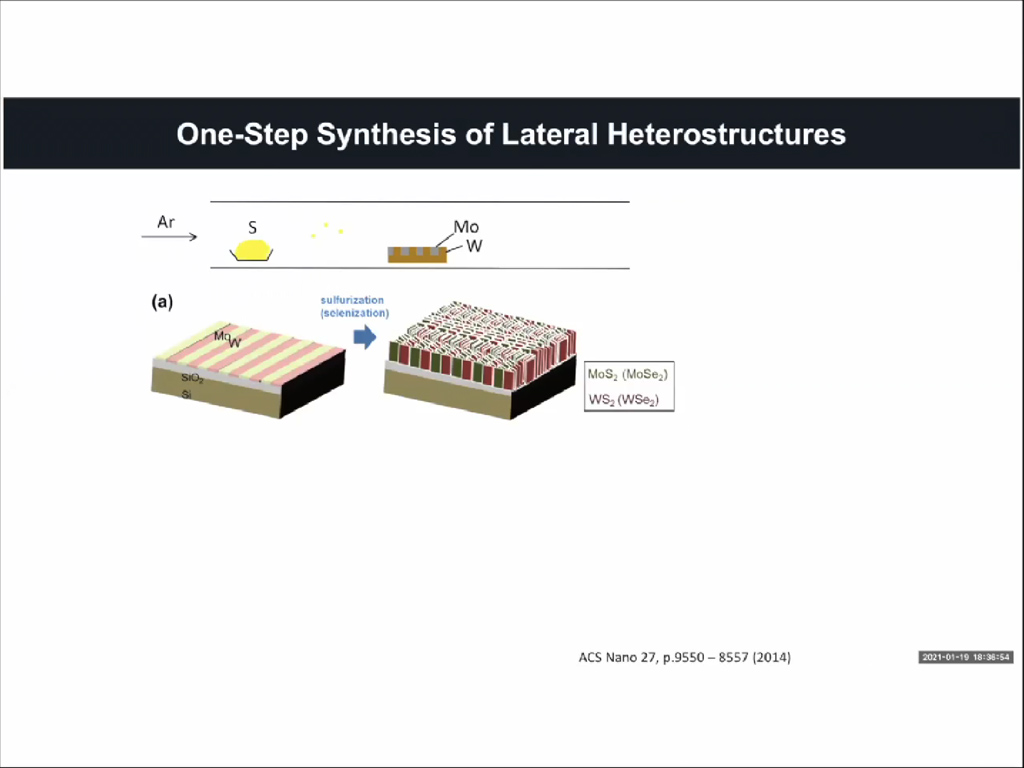
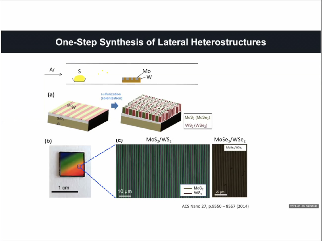
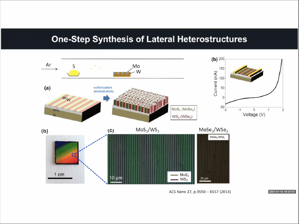 8. One-Step Synthesis of Lateral …
330.46379713046383
00:00/00:00
8. One-Step Synthesis of Lateral …
330.46379713046383
00:00/00:00 -
 9. One-Step Synthesis of Vertical…
398.66533199866535
00:00/00:00
9. One-Step Synthesis of Vertical…
398.66533199866535
00:00/00:00 -
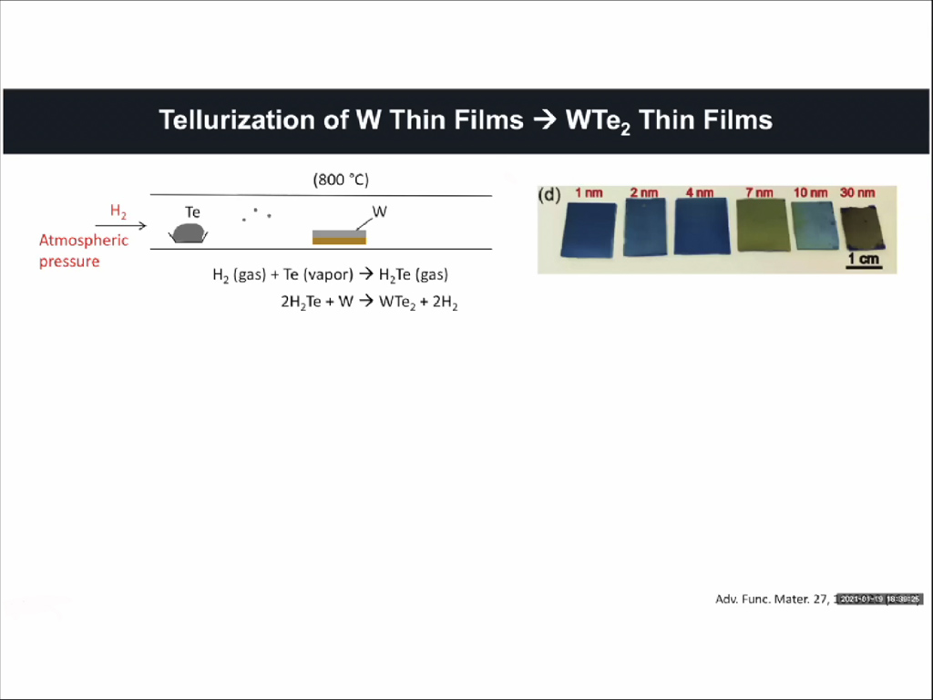
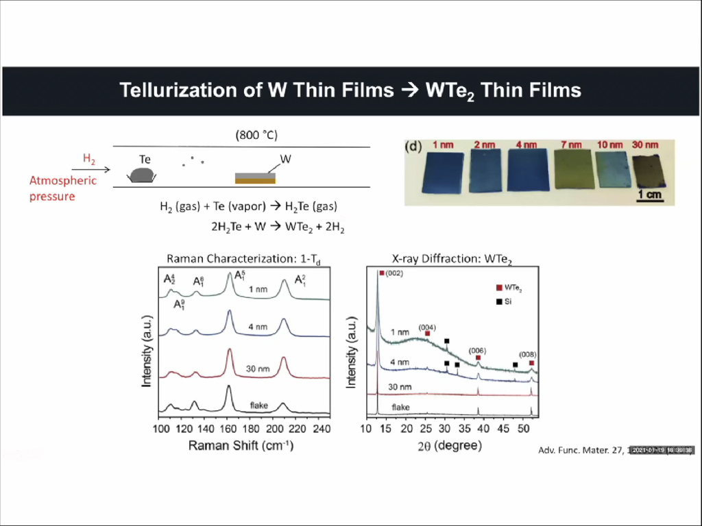 10. Tellurization of W Thin Films …
446.312979646313
00:00/00:00
10. Tellurization of W Thin Films …
446.312979646313
00:00/00:00 -
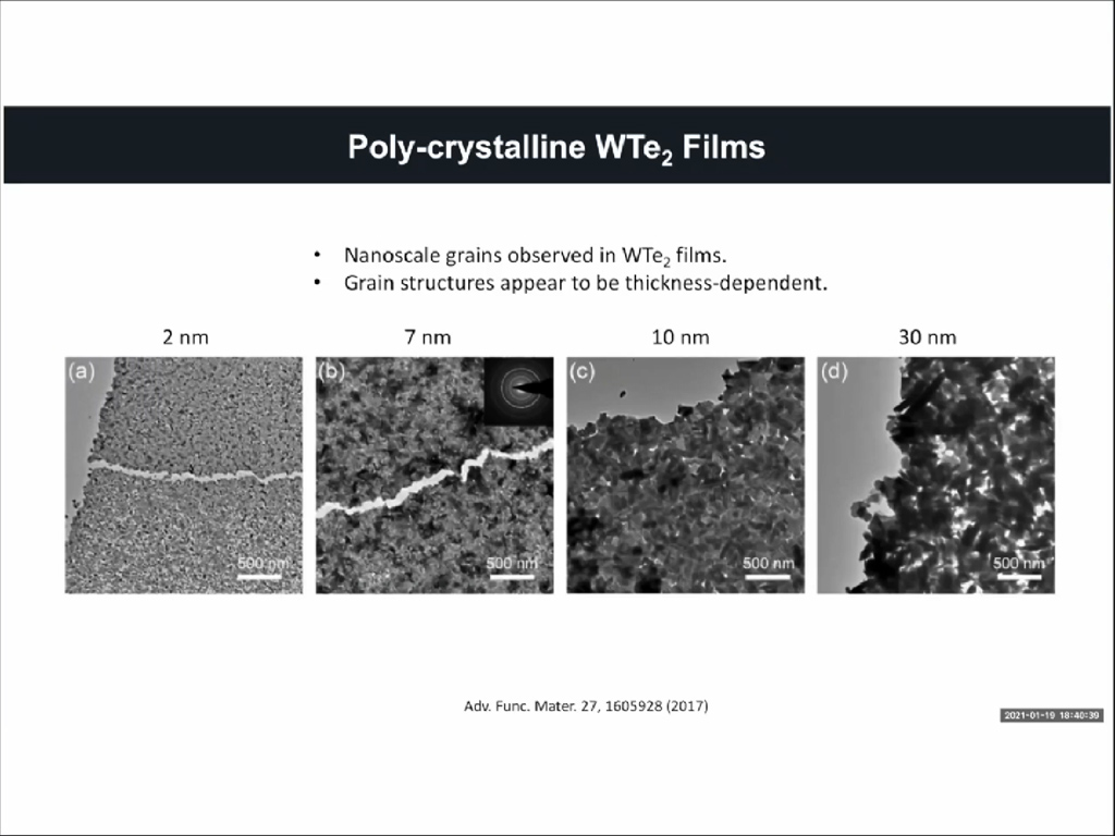 11. Poly-crystalline WTe2 Films
505.70570570570572
00:00/00:00
11. Poly-crystalline WTe2 Films
505.70570570570572
00:00/00:00 -
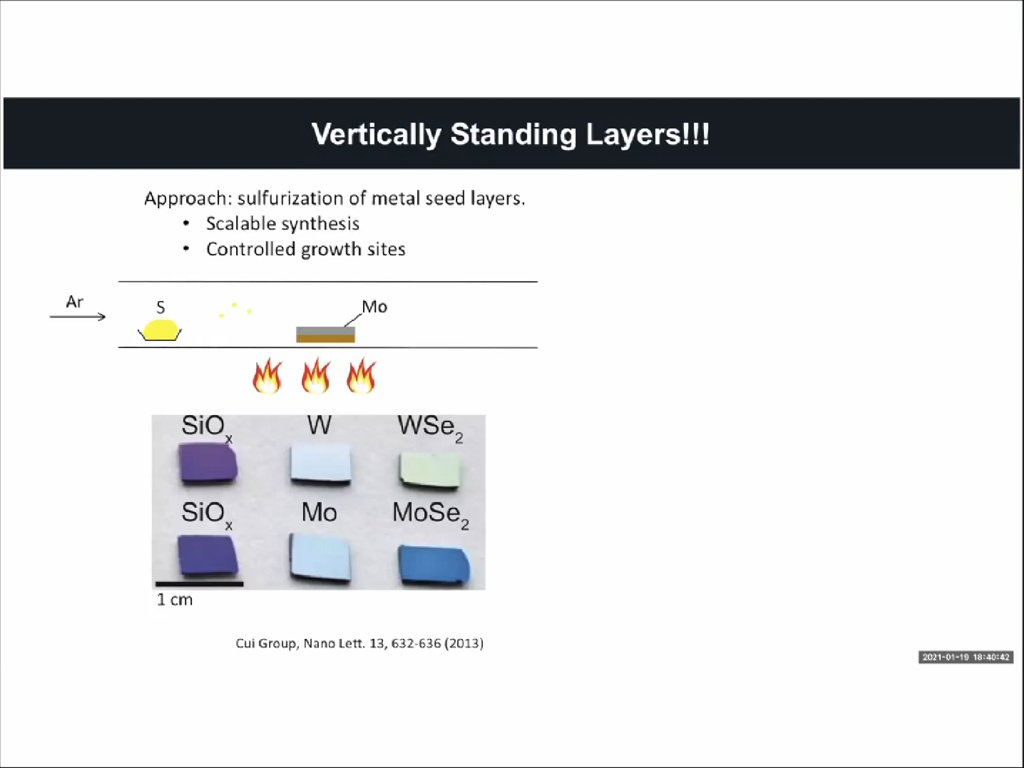
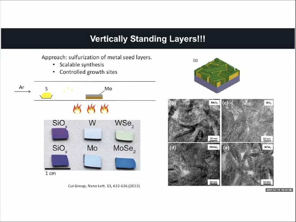 12. Vertically Standing Layers!!
556.3897230563897
00:00/00:00
12. Vertically Standing Layers!!
556.3897230563897
00:00/00:00 -
 13. Vertical to Horizontal Layer G…
606.74007340674007
00:00/00:00
13. Vertical to Horizontal Layer G…
606.74007340674007
00:00/00:00 -
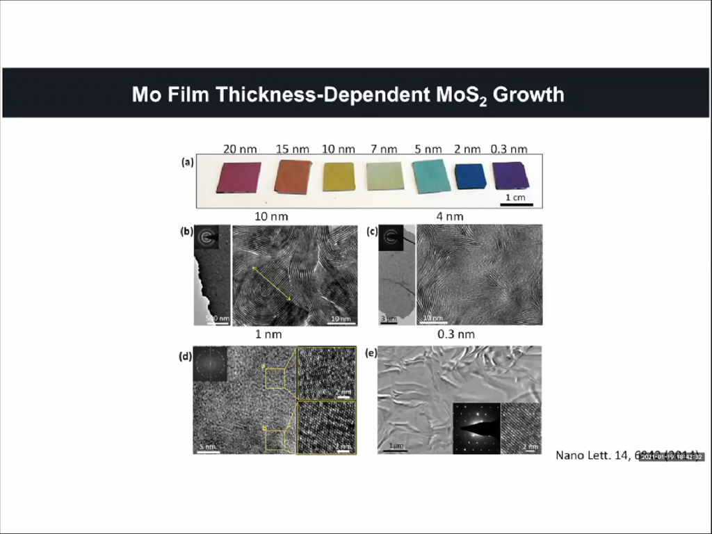 14. Mo Film Thickness-Dependent Mo…
662.92959626292964
00:00/00:00
14. Mo Film Thickness-Dependent Mo…
662.92959626292964
00:00/00:00 -
 15. W Film Thickness-Dependent Gro…
719.35268601935275
00:00/00:00
15. W Film Thickness-Dependent Gro…
719.35268601935275
00:00/00:00 -
 16. Volume Expansion and Strain Ef…
762.46246246246244
00:00/00:00
16. Volume Expansion and Strain Ef…
762.46246246246244
00:00/00:00 -
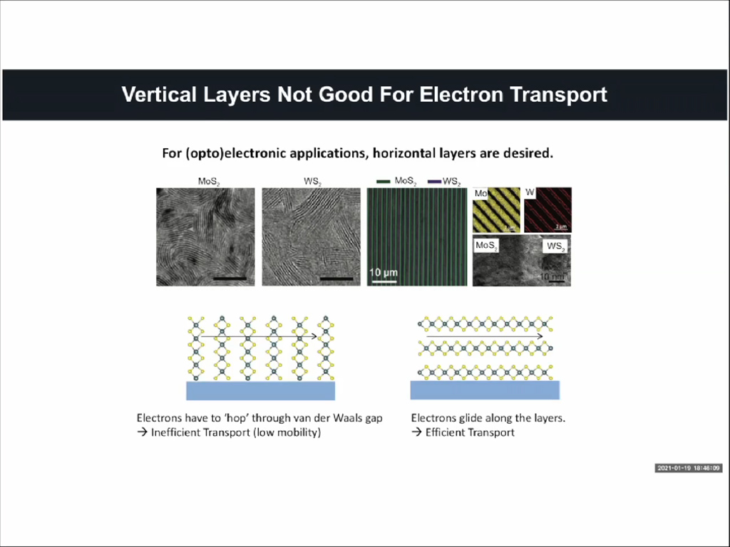 17. Vertical Layers Not Good for E…
854.98832165498834
00:00/00:00
17. Vertical Layers Not Good for E…
854.98832165498834
00:00/00:00 -
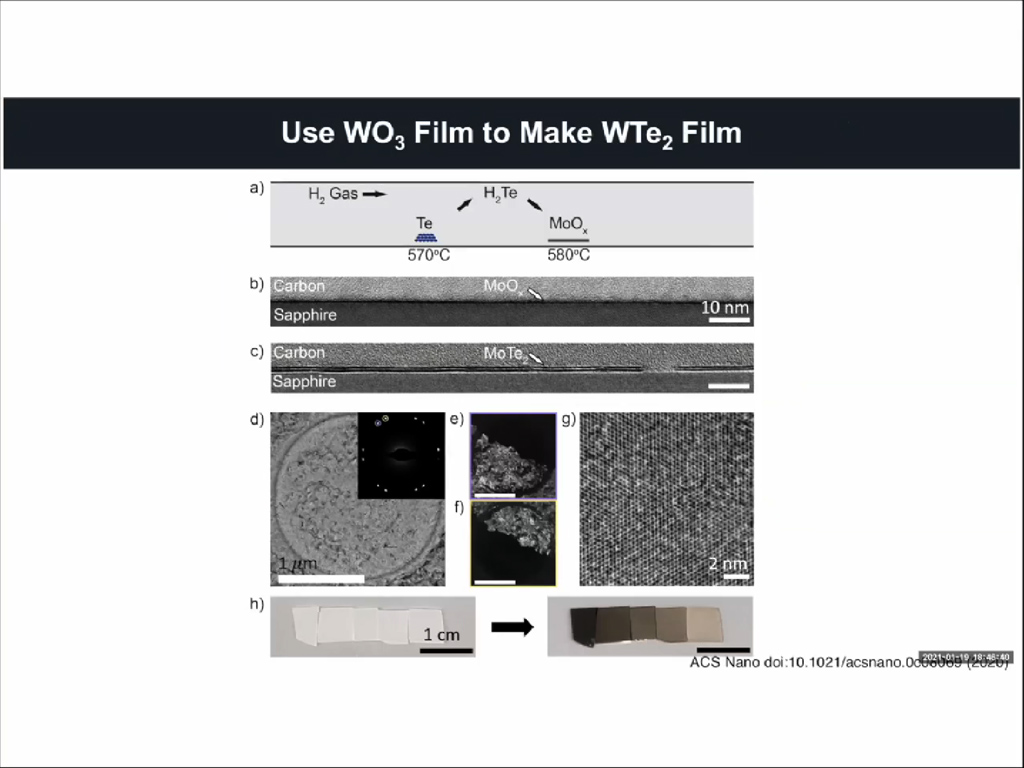 18. Use WO3 Film to Make WTe2 Film
912.545879212546
00:00/00:00
18. Use WO3 Film to Make WTe2 Film
912.545879212546
00:00/00:00 -
 19. ALD WO3 to Control Thickness o…
1023.923923923924
00:00/00:00
19. ALD WO3 to Control Thickness o…
1023.923923923924
00:00/00:00 -
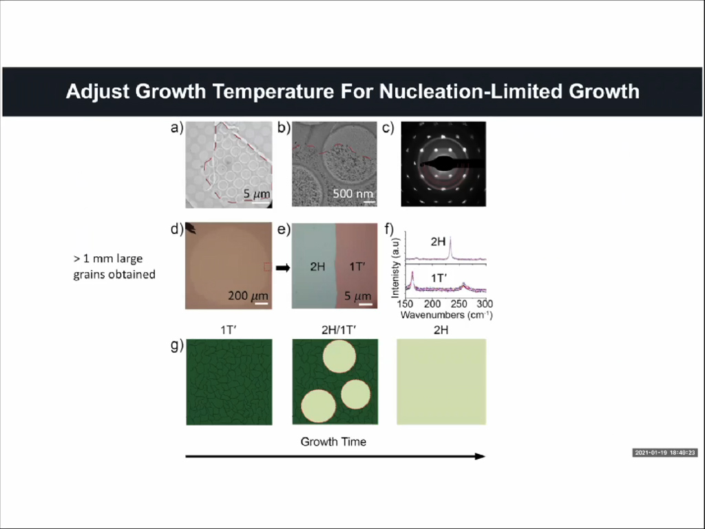 20. Adjust Growth Temperature for …
1076.8101434768103
00:00/00:00
20. Adjust Growth Temperature for …
1076.8101434768103
00:00/00:00 -
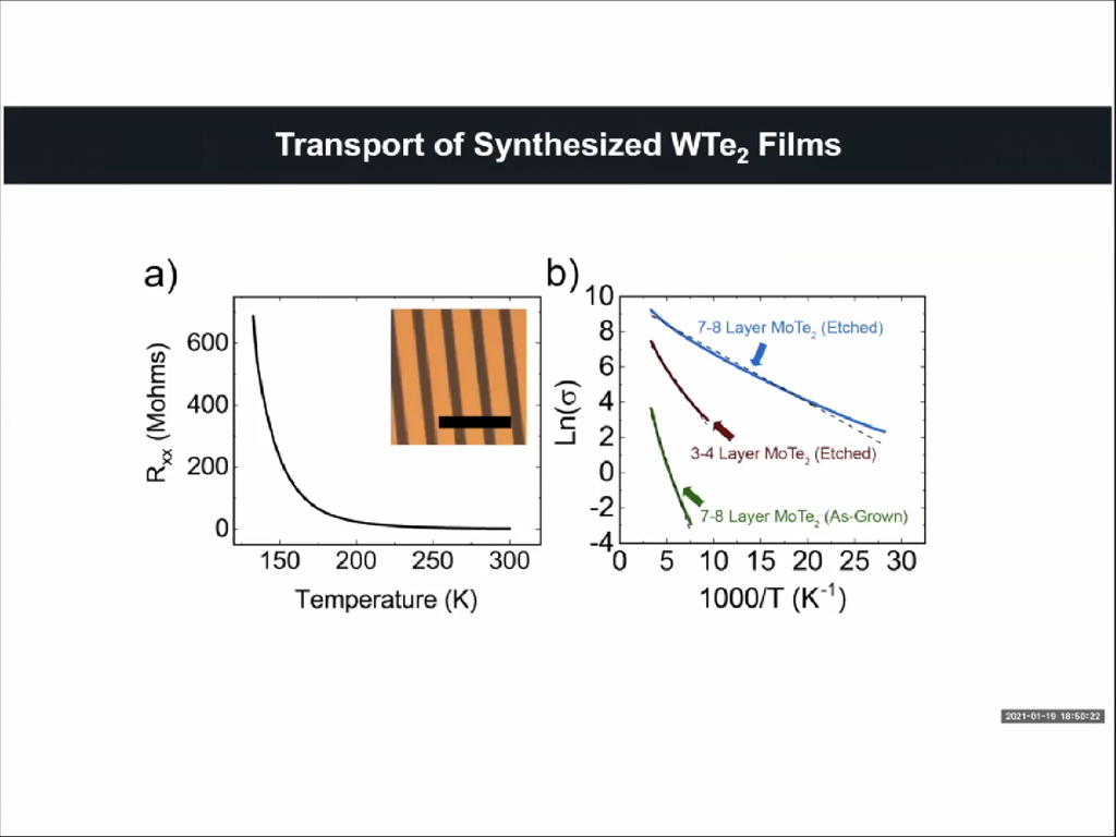 21. Transport of Synthesized WTe2 …
1137.203870537204
00:00/00:00
21. Transport of Synthesized WTe2 …
1137.203870537204
00:00/00:00 -
 22. Effects of Substrate on Film Q…
1205.6389723056391
00:00/00:00
22. Effects of Substrate on Film Q…
1205.6389723056391
00:00/00:00 -
 23. WO3 Nanowires -> WTe2 Nanowire…
1297.1971971971973
00:00/00:00
23. WO3 Nanowires -> WTe2 Nanowire…
1297.1971971971973
00:00/00:00 -
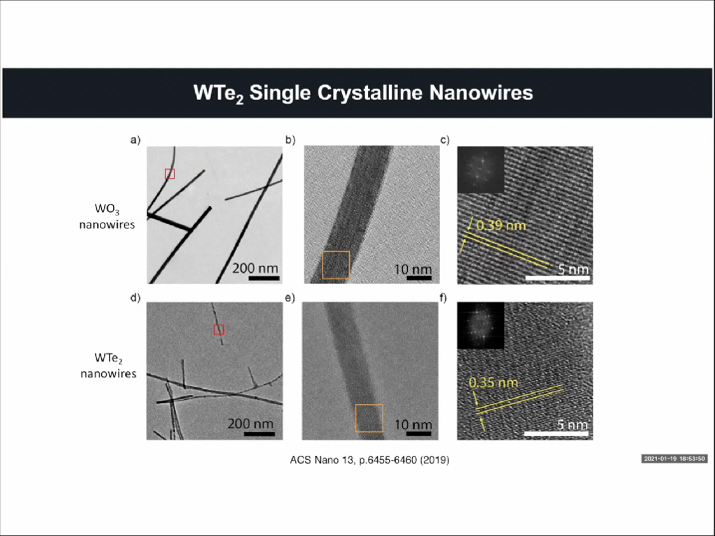 24. WTe2 Single Crystalline Nanowi…
1326.6933600266934
00:00/00:00
24. WTe2 Single Crystalline Nanowi…
1326.6933600266934
00:00/00:00 -
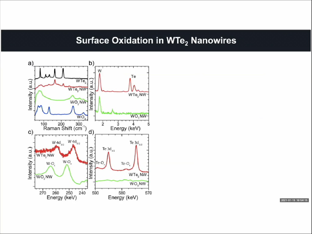
 25. Surface Oxidation in WTe2 Nano…
1370.3703703703704
00:00/00:00
25. Surface Oxidation in WTe2 Nano…
1370.3703703703704
00:00/00:00 -
 26. Synthesis of MoP Nanostructure…
1439.73973973974
00:00/00:00
26. Synthesis of MoP Nanostructure…
1439.73973973974
00:00/00:00 -
 27. MoP Nanowires for Interconnect…
1463.1297964631299
00:00/00:00
27. MoP Nanowires for Interconnect…
1463.1297964631299
00:00/00:00 -
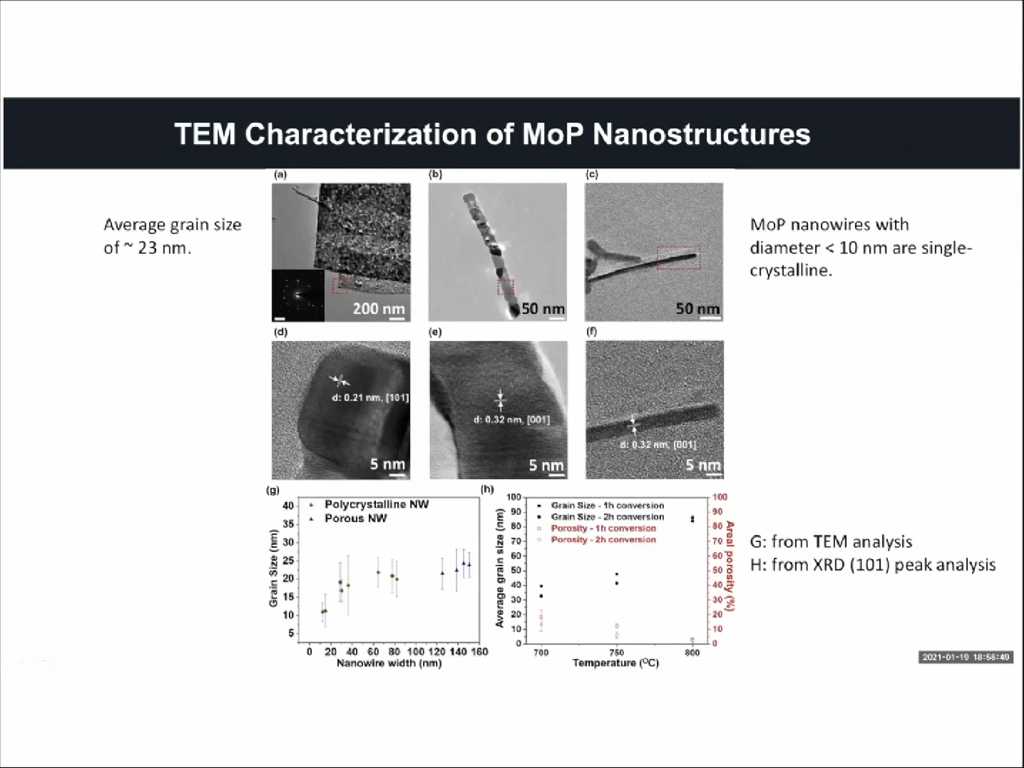 28. TEM Characterization of MoP Na…
1518.8521855188521
00:00/00:00
28. TEM Characterization of MoP Na…
1518.8521855188521
00:00/00:00 -
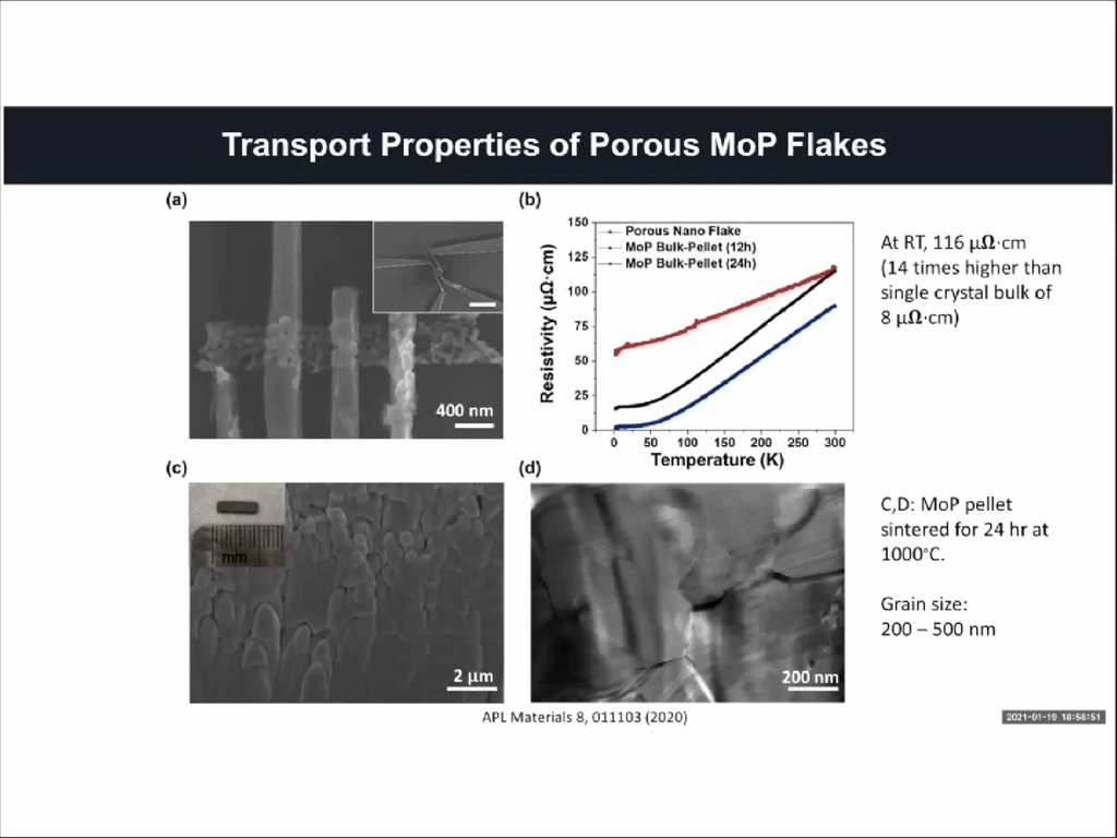 29. Transport Properties of Porous…
1519.3526860193526
00:00/00:00
29. Transport Properties of Porous…
1519.3526860193526
00:00/00:00 -
 30. Grain Size as Function of Nano…
1553.3533533533534
00:00/00:00
30. Grain Size as Function of Nano…
1553.3533533533534
00:00/00:00 -
 31. Outline
1564.4978311644979
00:00/00:00
31. Outline
1564.4978311644979
00:00/00:00 -
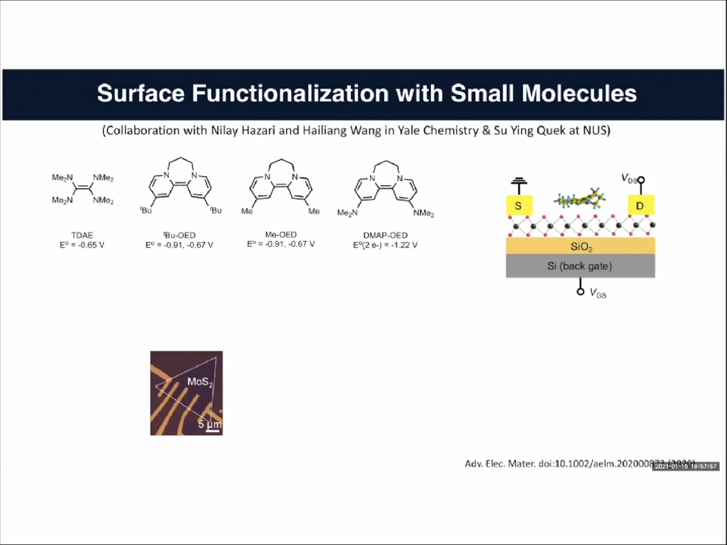
 32. Surface Functionalization with…
1580.980980980981
00:00/00:00
32. Surface Functionalization with…
1580.980980980981
00:00/00:00 -
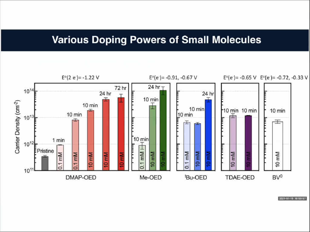 33. Various Doping Powers of Small…
1702.1354688021356
00:00/00:00
33. Various Doping Powers of Small…
1702.1354688021356
00:00/00:00 -
 34. 2D Material – Molecule Inter…
1714.3476810143477
00:00/00:00
34. 2D Material – Molecule Inter…
1714.3476810143477
00:00/00:00 -
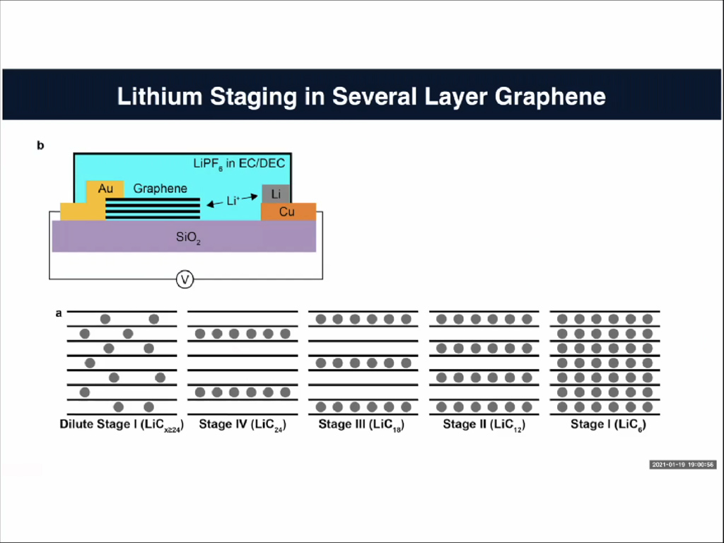
 35. Lithium Staging in Several Lay…
1744.2442442442443
00:00/00:00
35. Lithium Staging in Several Lay…
1744.2442442442443
00:00/00:00 -
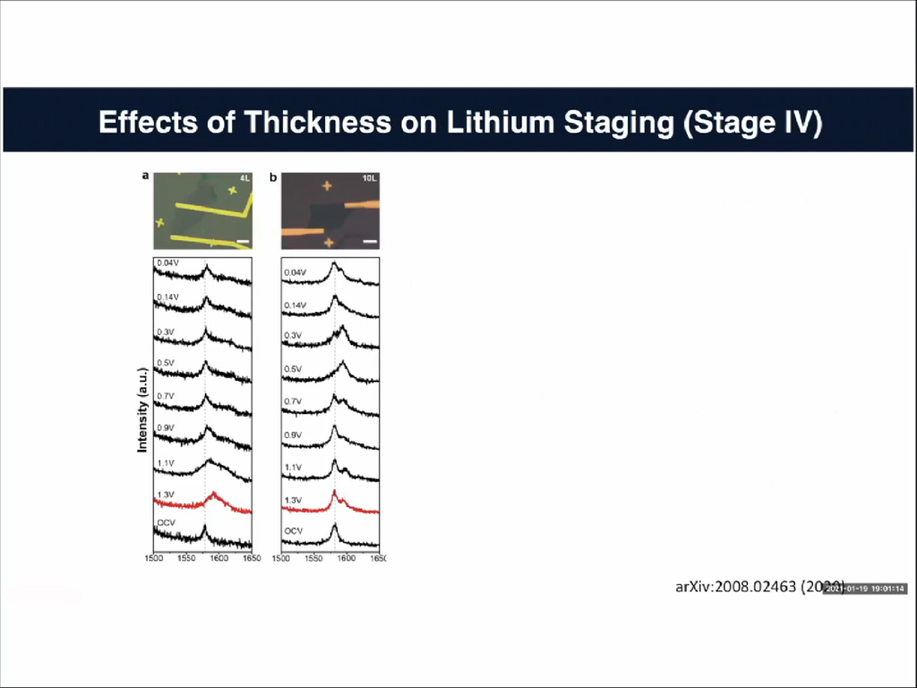
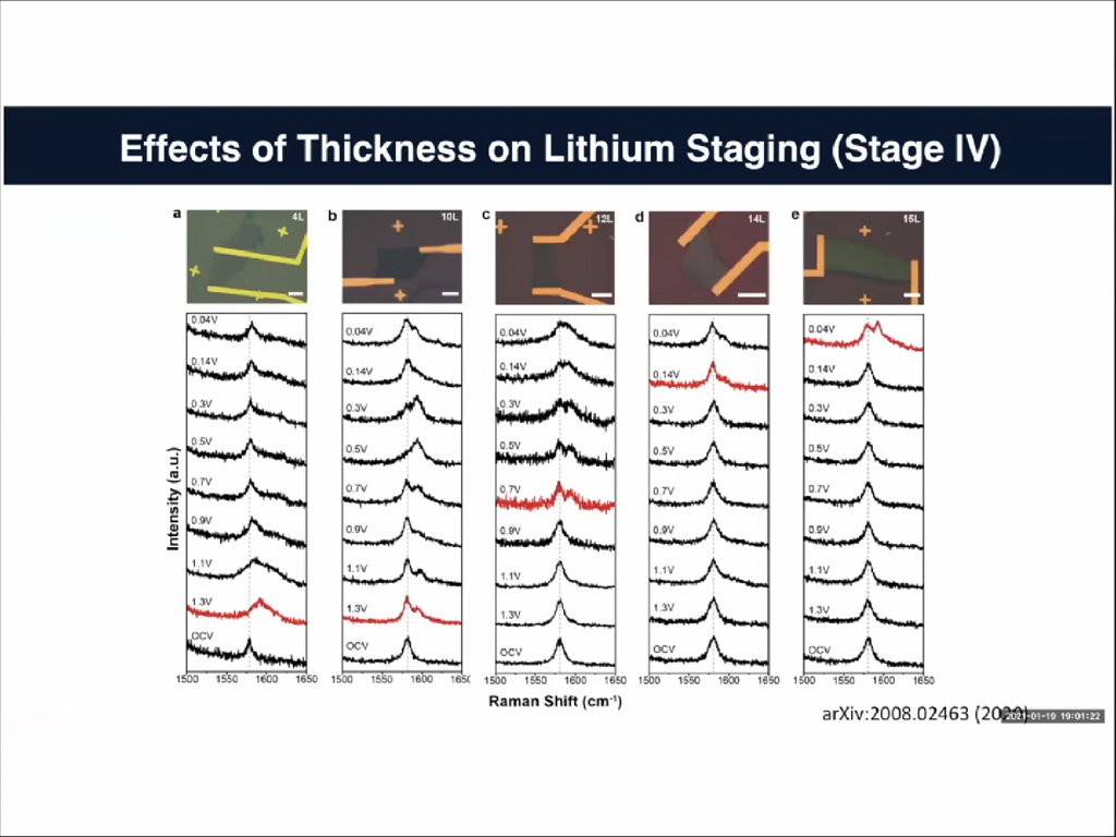 36. Effects of Thickness on Lithiu…
1780.4137470804137
00:00/00:00
36. Effects of Thickness on Lithiu…
1780.4137470804137
00:00/00:00 -
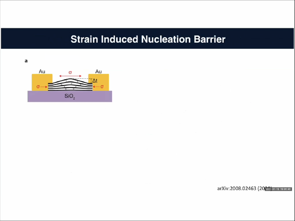
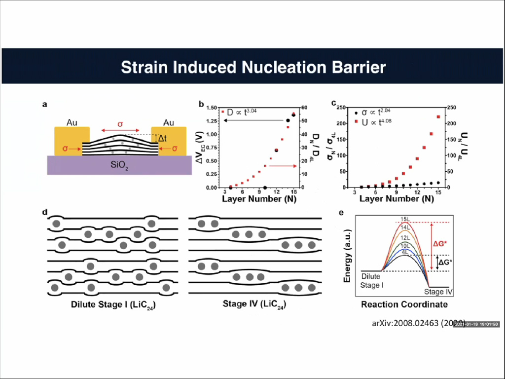 37. Strain Induced Nucleation Barr…
1810.2102102102103
00:00/00:00
37. Strain Induced Nucleation Barr…
1810.2102102102103
00:00/00:00 -
 38. Intercalation in hBN/MoS2/hBN …
1842.5425425425426
00:00/00:00
38. Intercalation in hBN/MoS2/hBN …
1842.5425425425426
00:00/00:00 -
 39. Summary
1851.0844177510844
00:00/00:00
39. Summary
1851.0844177510844
00:00/00:00 -
40. Use WO3 Film to Make WTe2 Film
1923.1231231231232
00:00/00:00
-
41. Vertical to Horizontal Layer G…
2336.2028695362028
00:00/00:00