A3 Crystalline Calcium Fluoride: A Record-Thin Insulator for Nanoscale 2D Electronics
Category
Published on
Abstract
Day 3 Session 3.2
Introduction: Two-dimensional (2D) electronics can enable FETs down to a few nanometers. However, these devices require scalable insulators which should form high-quality interfaces with 2D channels and maintain low gate leakage currents for sub-1nm equivalent oxide thickness (EOT). Previously used amorphous oxides result in poor interfaces with 2D materials, while hBN has mediocre dielectric properties (ε < 5, Eg = 6eV) [1]. As a promising alternative, we suggest the use of the crystalline ionic insulator CaF2 (ε = 8.43, Eg = 12.1eV) which forms van der Waals interfaces with 2D semiconductors [2]. At the moment, CaF2 can be grown by molecular-beam epitaxy (MBE) down to a few nanometers thickness [3] and appears promising for chemical vapour deposition (CVD) [4] and atomic-layer deposition (ALD) [5]. Here we discuss our recent progress [3, 6, 7] on ultra-thin CaF2 which presents a universal platform for 2D devices. In particular, we demonstrate nanoscale MoS2 FETs with L =50-60nm and a record-thin ∼2nm CaF2 insulator (EOT∼0.9nm) which exhibits near-ideal subthreshold swing (SS).
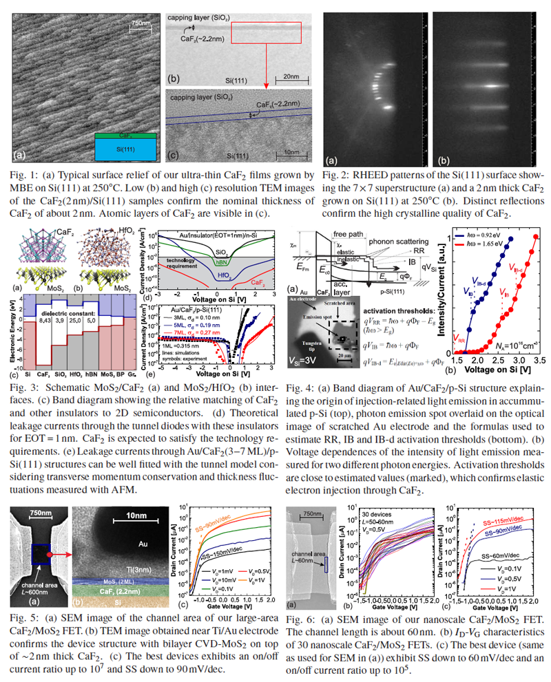
Growth and structure of CaF2 films: MBE of CaF2 on Si(111) has been known for over three decades [8]. However, previously used high-temperature growth (up to 800◦C), which targeted high crystallinity, results in the formation of triangular pinholes [9]. To address this problem, we have succeeded in growing CaF2 at 250◦C [6] after careful cleaning of Si(111) substrates [10]. This allowed us to obtain pinhole-free homogeneous CaF2 films with 1−2nm thickness. For instance, the atomic-force microscopy (AFM) image in Fig.1a shows that the surface of CaF2 is flat with clearly visible atomic steps, and the transmission electron microscopy (TEM) images from Fig.1b,c confirm that the 2nm thick CaF2 film consists of triple F-Ca-F monolayers (1ML=0.315nm, Fig.1c). Despite low-temperature MBE growth, reflection high energy electron diffraction (RHEED) patterns (Fig.2) contain distinct streaks which indicates high crystallinity of our CaF2 films grown on atomically clean Si(111).
High-quality CaF2 for device applications: An important advantage of CaF2 is its inert (111) surface which forms well-defined interfaces with 2D materials [2] (Fig.3a). This is in contrast to amorphous oxides like HfO2 which contain dangling bonds (Fig.3b). Also, CaF2 has a reasonably high permittivity (ε = 8.43), an extremelywide bandgap (Eg = 12.1eV) and forms high band offsets with Si and 2D semiconductors (Fig.3c). Thus, predicted leakage currents through CaF2 are lower [11] than those through HfO2, hBN and SiO2 (Fig.3d), and fit the end-of-roadmap requirement. To understand leakage mechanisms through CaF2,we measured the I−V curves of Au/CaF2/Si(111) diodes [3,6,12]. We found that the results can be reproduced with theoretical tunneling models considering thickness fluctuations [3] and transverse momentum conservation [12] (Fig.3e). The latter becomes important because of the (111) orientation and further suppresses tunneling through CaF2 [12]. Next we analyzed the light emission of hot electrons which are injected through CaF2 to p-Si under accummulation (VSi >0) and can be involved in recombination (RR), intra-band (IB) and intra-band direct (IB-d) radiative transitions (Fig.4a) [3,13]. We found that activation thresholds measured for different photon energies ħω are close to their estimated values (Fig.4b) and concluded that carrier injection through CaF2 is elastic, i.e. takes place without energy dissipations. This means that our CaF2 layers are mostly defect-free and thus perfectly suited for device applications.
MoS2 FETs with 2nm CaF2: Fig.5 demonstrates the use of Si(111)/CaF2 substrates for MoS2 FETs [7]. Devices have been produced by transferring bilayer CVD-grown MoS2 films onto CaF2 and shaping Ti/Au electrodes with ebeam lithography. First we fabricated hundreds of large-area (L =400 - 800nm) MoS2 FETs with 2nm thick CaF2 [7] and confirmed the device structure using scanning electron microscopy (SEM, Fig.5a) and TEM (Fig.5b). Then we found that the best devices exhibit SS down to 90mV/dec and record-high on/off current ratios up to 107 for 2nm thick insulators (Fig.5c). Finally, we extended the source Ti/Au area and shaped nanoscale CaF2/MoS2 FETs with L =50-60nm(Fig.6). These devices exhibit excellent drain current control by the gate bias VG and near-ideal SS down to 60mV/dec, which slightly degrades at larger VD where the device reaches the full on state.
Conclusions: We fabricated high-quality crystalline 1−2nm CaF2 films and successfully used them for MoS2 FETs with record-thin gate insulators. For the first time we demonstrated MoS2 FETs with simultaneously sub-1nm EOT insulators and sub-100nm channel length and found that these devices can exhibit near-ideal SS. Our results suggest that Si(111)/CaF2 substrates provide a universal platform for future 2D nanoelectronics, which has enormous potential due to the possibility of direct growth of 2D semiconductors on CaF2 [14]
Sponsored by
References
- G. Cassabois et al., Nat. Photon. 10, 262 (2016).
- A. Koma et al., Appl. Surf. Sci. 41, 451 (1990).
- Y. Illarionov et al., J. Appl. Phys. 115, 223706 (2014).
- A. Purdy et al., Inorg. Chem. 28, 2799 (1989).
- T. Pilvi et al., Chem.Mater. 19, 3387 (2007).
- M. Vexler et al., J. Appl. Phys. 105, 083716 (2009).
- Y. Illarionov et al., Nat. Electron. 2, 230 (2019).
- R. Farrow et al., J. Vac. Sci. Techn. 19, 415 (1981).
- S. Watanabe et al., Jpn. J. Appl. Phys. 44, 2637 (2005).
- A. Ishizaka et al., J. Electrochem. Soc. 133, 666 (1986).
- Y. Illarionov et al., Tech. Phys. Lett. 36, 404 (2010).
- Y. Illarionov et al., Microelectron. Eng. 88, 1291 (2011).
- Y. Illarionov et al., Thin Solid Films 545, 580 (2013).
- S. Vishwanath et al., J. Cryst. Growth 482, 61 (2018).
Cite this work
Researchers should cite this work as follows:
-
Yury Yuryevich Illarionov, A.G. Banshchikov, Theresia Knobloch, D.K. Polyushkin, S. Wachter, V.V. Fedorov, M. Stöger-Pollach, M.I. Vexler, N.S. Sokolov, T. Grasser (2020), "A3 Crystalline Calcium Fluoride: A Record-Thin Insulator for Nanoscale 2D Electronics," https://nanohub.org/resources/34171.
Time
Location
DRC 2020 Virtual Conference