Density Functional Tight Binding (DFTB) Modeling in the Context of Ultra-Thin Silicon-on-Insulator MOSFETs
Density Functional Tight Binding (DFTB) Modeling in the Context of Ultra-Thin Silicon-on-Insulator MOSFETs
-
 1. Density functional tight bindi…
0
00:00/00:00
1. Density functional tight bindi…
0
00:00/00:00 -
 2. From atom to transistor: Can w…
26.493159826493162
00:00/00:00
2. From atom to transistor: Can w…
26.493159826493162
00:00/00:00 -
 3. State of the art atomistic mod…
58.858858858858859
00:00/00:00
3. State of the art atomistic mod…
58.858858858858859
00:00/00:00 -
 4. General approach and choice of…
132.69936603269937
00:00/00:00
4. General approach and choice of…
132.69936603269937
00:00/00:00 -
 5. Outline
178.74541207874543
00:00/00:00
5. Outline
178.74541207874543
00:00/00:00 -
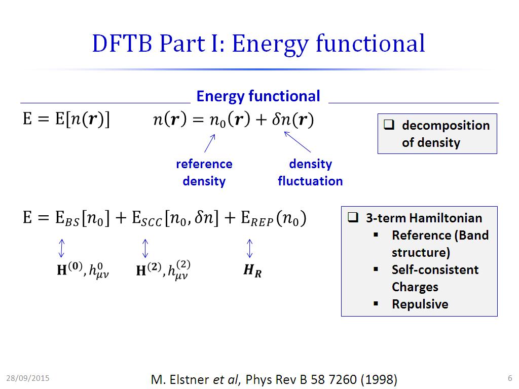 6. DFTB Part I: Energy functional
198.43176509843178
00:00/00:00
6. DFTB Part I: Energy functional
198.43176509843178
00:00/00:00 -
 7. DFTB Part II: Reference Hamilt…
245.54554554554557
00:00/00:00
7. DFTB Part II: Reference Hamilt…
245.54554554554557
00:00/00:00 -
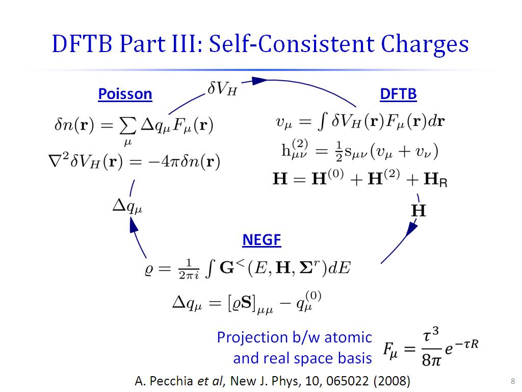 8. DFTB Part III: Self-Consistent…
309.3093093093093
00:00/00:00
8. DFTB Part III: Self-Consistent…
309.3093093093093
00:00/00:00 -
 9. DFTB ...take away message
403.26993660326997
00:00/00:00
9. DFTB ...take away message
403.26993660326997
00:00/00:00 -
 10. DFTB parameterisation for Si: …
443.54354354354354
00:00/00:00
10. DFTB parameterisation for Si: …
443.54354354354354
00:00/00:00 -
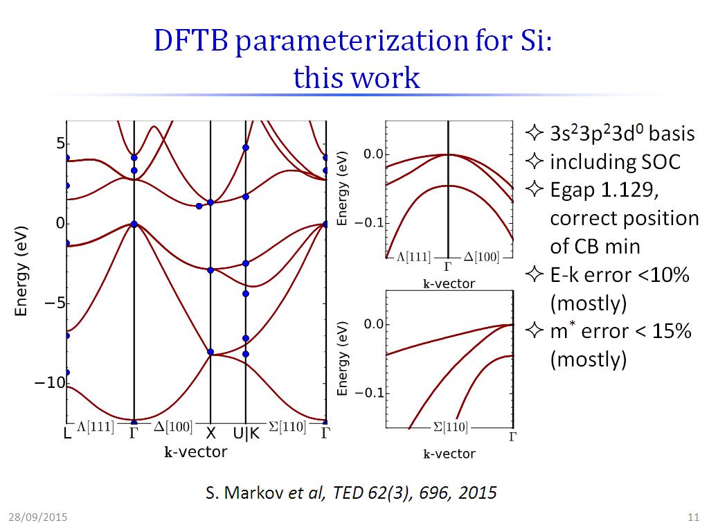 11. DFTB parameterization for Si: …
457.45745745745745
00:00/00:00
11. DFTB parameterization for Si: …
457.45745745745745
00:00/00:00 -
 12. DFTB parameterisation for Alph…
463.93059726393062
00:00/00:00
12. DFTB parameterisation for Alph…
463.93059726393062
00:00/00:00 -
 13. Atomic models for SOI: Si/SiO2…
485.91925258591925
00:00/00:00
13. Atomic models for SOI: Si/SiO2…
485.91925258591925
00:00/00:00 -
 14. Si Band-gap vs Si film thickne…
522.98965632298973
00:00/00:00
14. Si Band-gap vs Si film thickne…
522.98965632298973
00:00/00:00 -
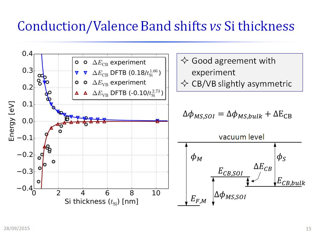 15. Conduction/Valence Band shifts…
557.82449115782447
00:00/00:00
15. Conduction/Valence Band shifts…
557.82449115782447
00:00/00:00 -
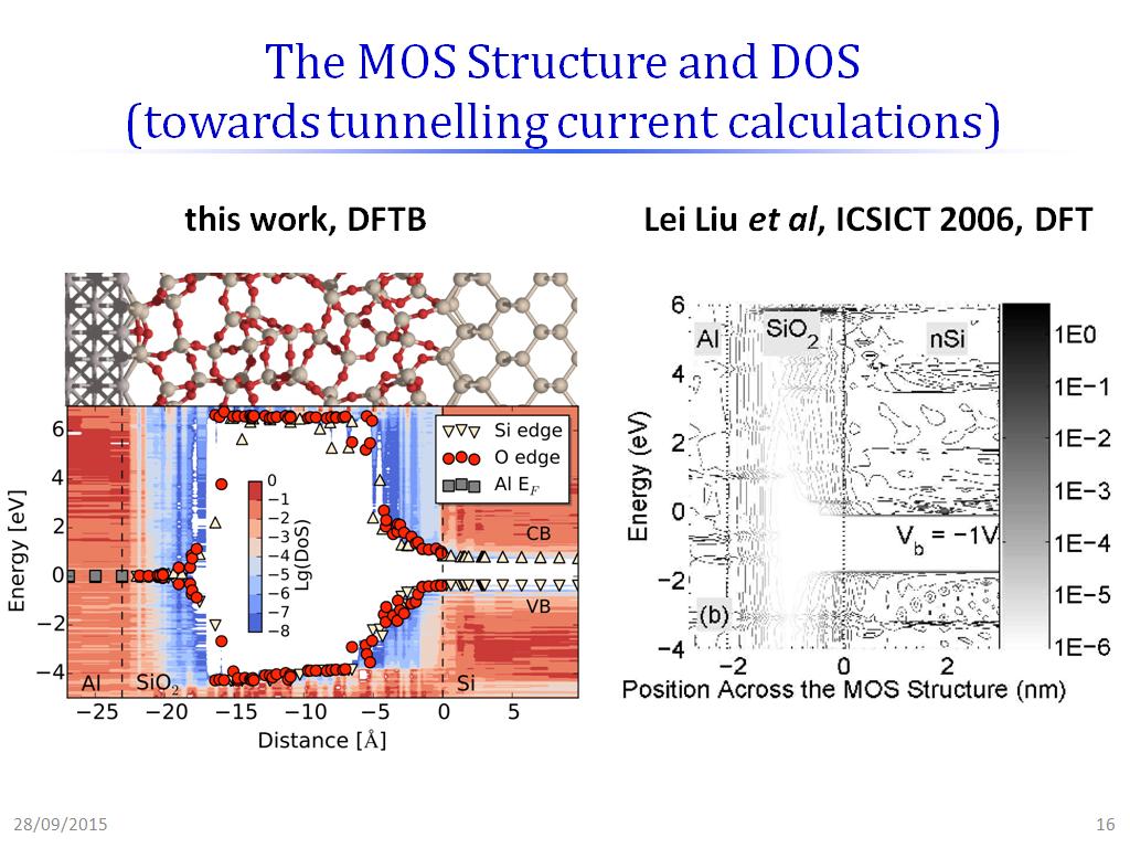 16. The MOS Structure and DOS (tow…
594.46112779446116
00:00/00:00
16. The MOS Structure and DOS (tow…
594.46112779446116
00:00/00:00 -
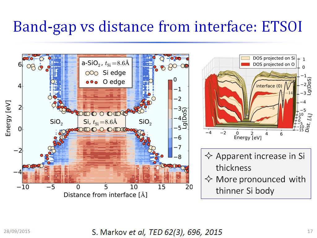 17. Band-gap vs distance from inte…
632.16549883216555
00:00/00:00
17. Band-gap vs distance from inte…
632.16549883216555
00:00/00:00 -
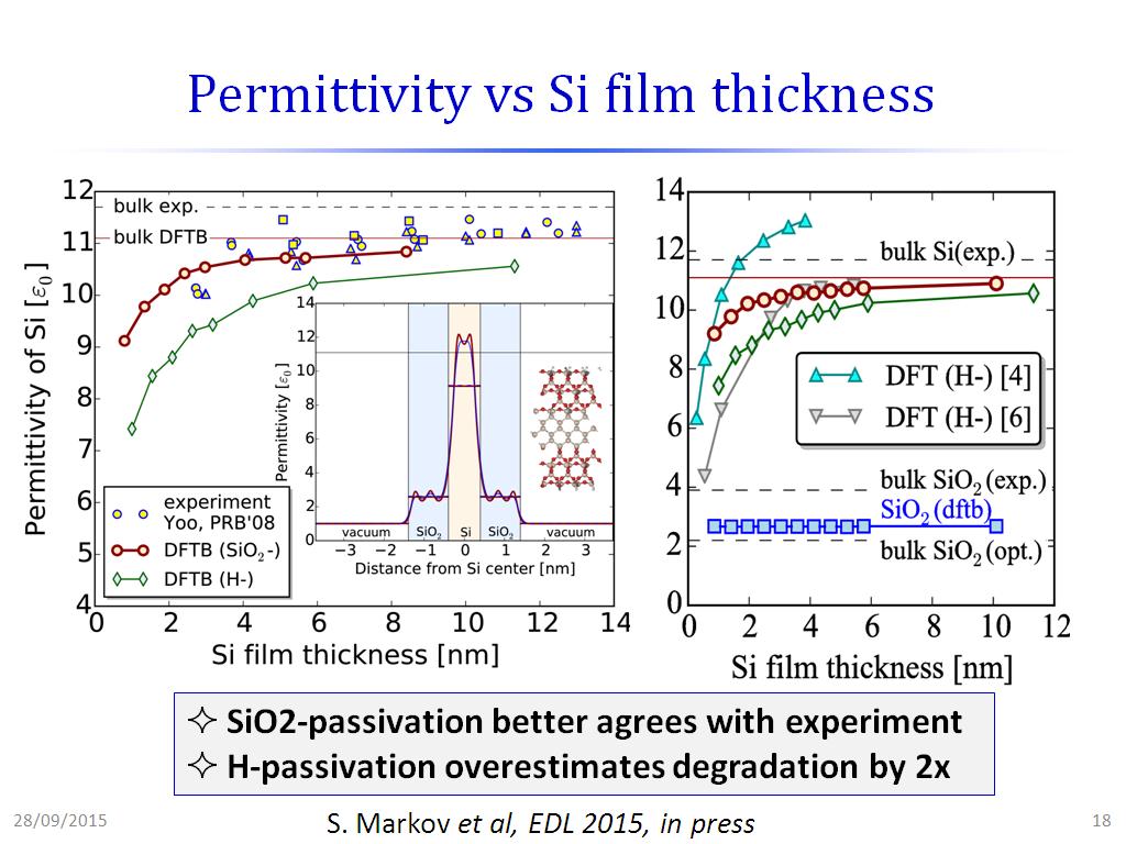 18. Permittivity vs Si film thickn…
646.84684684684692
00:00/00:00
18. Permittivity vs Si film thickn…
646.84684684684692
00:00/00:00 -
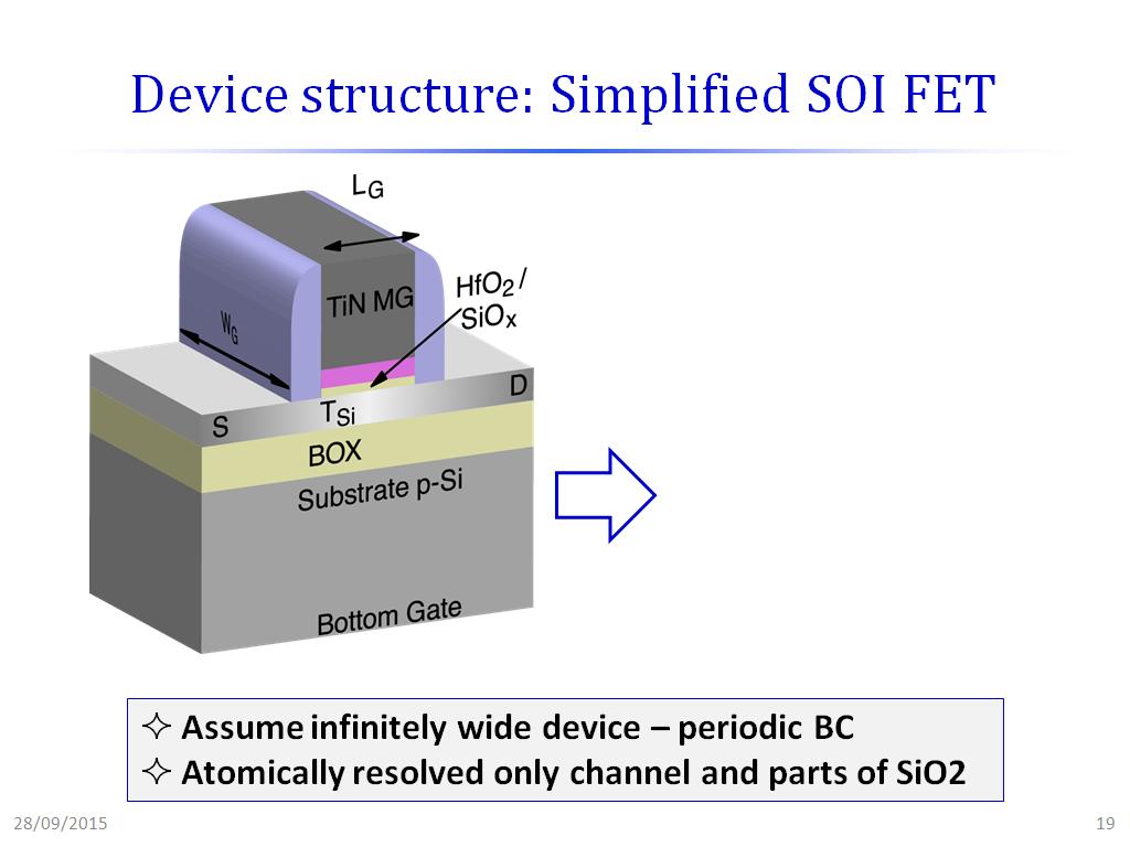
 19. Device structure: Simplified …
724.89155822489158
00:00/00:00
19. Device structure: Simplified …
724.89155822489158
00:00/00:00 -
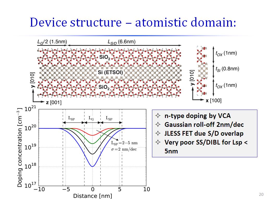 20. Device structure – atomistic…
777.84451117784454
00:00/00:00
20. Device structure – atomistic…
777.84451117784454
00:00/00:00 -
 21. IDVG – H- vs SiO2-passivatio…
808.641975308642
00:00/00:00
21. IDVG – H- vs SiO2-passivatio…
808.641975308642
00:00/00:00 -
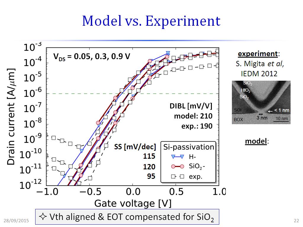
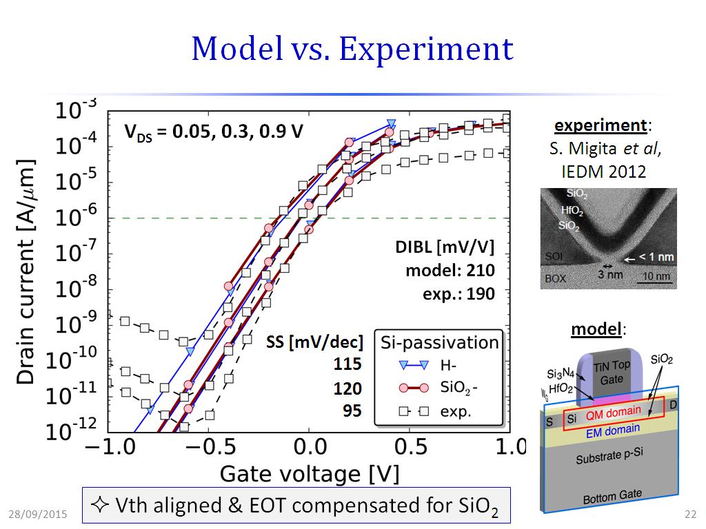 22. Model vs. Experiment
867.80113446780115
00:00/00:00
22. Model vs. Experiment
867.80113446780115
00:00/00:00 -
 23. Conclusions
929.99666332999675
00:00/00:00
23. Conclusions
929.99666332999675
00:00/00:00 -
 24. Acknowledgements
965.76576576576576
00:00/00:00
24. Acknowledgements
965.76576576576576
00:00/00:00