Quantum Dot Wave Function (Quantum Dot Lab)
Category
Published on
Abstract
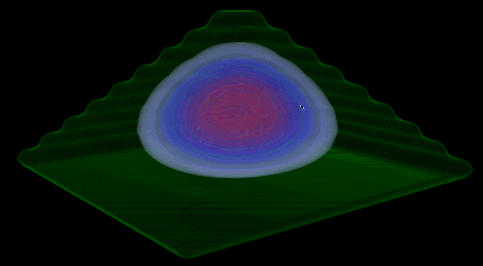
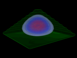 Electron density of an artificial atom. Specifically, the animation sequence shows various electronic states in an Indium Arsenide (InAs)/Gallium Arsenide (GaAs) self-assembled quantum dot. The nanometer-scaled structure of the semiconductor InAs embedded in GaAs can confine electrons much like a proton can attract an electron in a hydrogen atom. This artificial atom is 100 times larger than a natural atom, and its properties can be manipulated by material composition, size and shape.
The semiconductor InAs can be grown as a crystal on top of a GaAs substrate. Since the natural InAs lattice constant is larger than that of GaAs, the material can clump up to form perfect crystal structures at nanoscale, that can take on pyramidal or dome shapes. The typical sizes of these quantum dots are 20nm in diameter and 5nm in height. The InAs material is typically capped and overgrown with GaAs. The central structure can confine additional electrons and form an artificial atom. These artificial atoms have the ability to absorb and emit light similar to natural atoms. The frequency or wavelength of this optical activity can be designed by quantum dot size, shape and material composition.
The animation sequence shows various electronic state wavefunctions starting from the s-like ground state, px, py-like excited states and additional more strangely looking excited states. These wavefunctions are computed in a simple effective mass model in the Quantum Dot Lab, powered by the Nanoelectronic Modeling Tool (NEMO 3D) and visualized with the nanoVIZ tool on nanoHUB.org.
Credits
Purdue University
References
- NEMO-3D
Gerhard Klimeck, Shaikh Ahmed, Hansang Bae, Neerav Kharche, Steve Clark, Benjamin Haley, Sunhee Lee, Maxim Naumov, Hoon Ryu, Faisal Saied, Marta Prada, Marek Korkusinski, and Timothy B. Boykin, "Atomistic Simulation of Realistically Sized Nanodevices Using NEMO 3-D: Part I - Models and Benchmarks", Special Issue on Nanoelectronic Device Modeling in IEEE Transactions on Electron Devices, Vol. 54, Issue 9, pg. 2079 - 2089 (2007). (available on nanoHUB.org) - nanoVIZ:
Wei Qiao, Michael Mclennan, Rick Kennell, David Ebert, and Gerhard Klimeck, "Hub-based Simulation and Graphics Hardware Accelerated Visualization for Nanotechnology Applications", IEEE Transactions on Visualization and Computer Graphics, Vol. 12, pg. 1061-1068 (2006). - nanoHUB.org:
Alejandro Strachan, Gerhard Klimeck, Mark S. Lundstrom, "Cyber-Enabled Simulations in Nanoscale Science and Engineering", Computing in Science and Engineering, Vol. 12, pg: 12-17 (2010). (available on nanoHUB.org) - Quantum Dot Lab:
Gerhard Klimeck; Lars Bjaalie; Sebastian Steiger; David Ebert; Tillmann Christoph Kubis; Matteo Mannino; Michael McLennan; Hong-Hyun Park; Michael Povolotskyi (2005), "Quantum Dot Lab," DOI: 10254/nanohub-r450.10.
Cite this work
Researchers should cite this work as follows: