Self-Assembled Quantum Dot Wave Structure
Category
Published on
Abstract
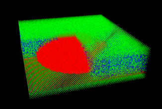 The semiconductor InAs can be grown as a crystal on top of a GaAs substrate. Since the natural InAs lattice constant is larger than the one of GaAs the material can clump up to form nanoscale, perfect crystal structures that can take on pyramidal or dome shapes. Typical sizes of such quantum dots are 20nm in diameter and 5nm in height. The InAs material is typically capped / overgrown with GaAs. Here an InAlAs overgrowth is shown. Such overgrowth is used to tune the optical emission properties of the embedded InAs quantum dot. The central structure can confine additional electrons and form an artificial atom. Such artificial atoms can have optical properties like natural atoms like the ability to absorb and emit light. The frequency or wavelength of this optical activity can be designed by quantum dot size, shape and material composition. The image shows an excited electron state in such InAs quantum dot. The electron density is colored by the orbital-resolved s, p, d character of the electron wavefunction contribution.
The atomistic structure was computed with the Nanoelectronic Modeling Tool (NEMO 3D) and visualized with the nanoVIZ tool on nanoHUB.org.
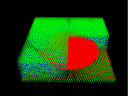 The image here is a 20nm wide and 5nm high dome shaped InAs quantum dot grown on GaAs and embedded in InAlAs. In atoms are shown in red, Ga atoms in green, and Al atoms in blue. As atoms are on a regular zinclblende lattice and are omitted for clarity. The central InAs contains about 100,000 atoms and forms an artificial atom that can confine electrons just like a natural atom.
Credits
Purdue University
References
- Quantum Dot Design:
Muhammad Usman, Hoon Ryu, Insoo Woo, David S. Ebert, and Gerhard Klimeck, "Moving towards nano-TCAD through multi-million atom quantum dot simulations matching experimental data" , IEEE Transactions on Nanotechnology, Vol. 8, Issue 3, pg. 330-344 (2009), DOI: 10.1109/TNANO.2008.2011900 (2009). - NEMO3D tool: on nanoHUB.org:
Gerhard Klimeck, Shaikh Ahmed, Hansang Bae, Neerav Kharche, Steve Clark, Benjamin Haley, Sunhee Lee, Maxim Naumov, Hoon Ryu, Faisal Saied, Marta Prada, Marek Korkusinski, and Timothy B. Boykin, "Atomistic Simulation of Realistically Sized Nanodevices Using NEMO 3-D: Part I - Models and Benchmarks", Special Issue on Nanoelectronic Device Modeling in IEEE Transactions on Electron Devices, Vol. 54, Issue 9, pg. 2079 - 2089 (2007). - nanoVIZ:
Wei Qiao, Michael Mclennan, Rick Kennell, David Ebert, and Gerhard Klimeck, "Hub-based Simulation and Graphics Hardware Accelerated Visualization for Nanotechnology Applications", IEEE Transactions on Visualization and Computer Graphics, Vol. 12, pg. 1061-1068 (2006). - nanoHUB.org:
Alejandro Strachan, Gerhard Klimeck, Mark S. Lundstrom, "Cyber-Enabled Simulations in Nanoscale Science and Engineering INTRODUCTION", Vol. 12, pg: 12-17 (2010).
Cite this work
Researchers should cite this work as follows: