Overview
![]()
This effort is supported by the NEEDS initiative to advance device science and connect it to applications
Introduction
Next-generation information technologies will process unprecedented amounts of loosely-structured data, including streaming video and audio, natural languages, real-time sensor readings, and contextual environments. These newly available data far exceed the processing capacity of known computing architectures and algorithms, thereby making coming generations of end-user applications infeasible. In particular, abundant-data applications expose gross inefficiencies in traditional architectures, where poor locality leads to excessive cache misses, causing massive and slow off-chip traffic to pin-limited DRAM memories that face their own scaling challenges. Thus, only small fractions of time and energy are responsible for computation itself – an opportunity for major improvements.

To overcome these challenges, and integrated approach for a new “nanosystem” technology capitalizes on several recent technology breakthroughs to enable massive energy efficiency and performance benefits for future abundant-data applications. The key components of nanosystems are:
-
High-performance and energy-efficient field-effect transistors (FETs) based on emerging atomic-scale nanomaterials, such as one-dimensional (1D) carbon nanotubes (CNTs) and two-dimensional (2D) semiconductors.
-
Massive amounts of high-density and energy-efficient non-volatile storage such as low-voltage Resistive RAM (RRAM) and magnetoresistive memories such as Spin-transfer torque magnetic RAM (STTMRAM). These diverse technologies offer complementary tradeoffs between high density, quick access, long data retention, and read/write endurance. Their advantages can be successfully utilized and their drawbacks avoided through a carefully-designed memory hierarchy and tight integration with computation units.
-
Fine-grained monolithic three-dimensional (3D) integration of computing and memory elements, layer by layer, with ultra-dense connectivity between layers. Such fine-grained monolithic 3D integration is natural to the N3XT transistor and memory technologies, enabled by low-temperature layer transfer techniques. This unique approach allows us to decouple high-temperature nanomaterial synthesis (to achieve high-quality materials) from low-temperature monolithic 3D integration.
-
Embedded cooling technologies targeting a range of application domains (e.g., hand-held vs. servers) to overcome power density challenges. Examples include conduction using 2D materials, management of thermal transients based on phase-change, and convective copper nanomesh structures connected to chip periphery microfluidics.
-
New microarchitectures and system runtimes for scalable computation immersed in memory that lead to massive amounts of active data, enabled by the above technology components and their fine-grained integration.

The design kit available on this site (i.e., the Nanosystem Design Kit, NDK) enables designers to create full physical designs for such nanosystems. The NDK leverages compact models also available on NEEDS, which are essential for designing such nanosystems. In contrast to previous work, the NDK does not perform circuit “benchmarking”, in which small circuit modules are analyzed using different compact models to evaluate which gives the best performance. Instead, the NDK highlights three key aspects about nanosystem design:
-
New applications drive the need for heterogeneous integration of multiple emerging nanotechnologies simultaneously, driving the need for multiple compact models.
-
Compact models ALONE are insufficient to design these nanosystems; at the system level, there are many effects that are not visible in small circuit benchmarks, including (but not limited to): wire parasitics, application-dependent workloads, cache architecture, and memory access patterns. Thus, the NDK highlights the need for higher-level models that take such system-level effects into consideration.
-
Many emerging nanotechnologies exhibit substantial variations, which can lead to significantly reduced circuit yield, increased susceptibility to noise, and large variations in circuit delays, and thus, techniques for overcoming variations are essential to realize nanosystem energy efficiency benefits.

In particular, the NDK illustrates the design of the OpenSparc T2 System on Chip (SoC), a large multicore chip that closely resembles the commercial Oracle/SUN Niagara 2 system, using Carbon Nanotube FETs (CNFETs) in the presence of variations. The circuit modules in OpenSparc T2 consist of ∼4,000 to >100,000 logic gates and expose several effects in VLSI-scale circuits (e.g., wire parasitics) that are not visible in small circuit benchmarks. The NDK demonstrates circuit design using CNFETs since they are excellent candidates for continuing to improve both performance and energy efficiency of digital systems. Furthermore, CNFETs provide an exciting opportunity to enable monolithic 3-D integrated circuits, leading to additional EDP benefits for CNFET-based digital systems with massive integration of logic and memory.
However, carbon nanotubes (CNTs) are inherently subject to variations that reduce circuit yield, increase susceptibility to noise, and severely degrade their anticipated energy and speed benefits. Joint exploration and optimization of CNT processing options and CNFET circuit design is required to overcome this outstanding challenge. Unfortunately, existing approaches for such exploration and optimization are computationally expensive, and mostly rely on trial-and-error-based ad hoc techniques. The tools available on this site provide a framework that quickly evaluates the impact of CNT variations on circuit delay and noise margin, and systematically explore the large space of CNT processing options to derive optimized CNT processing and CNFET circuit design guidelines. This framework: 1) runs over 100x faster than existing approaches and 2) accurately identifies the most important CNT processing parameters, together with CNFET circuit design parameters (e.g., for CNFET sizing and standard cell layouts), to minimize the impact of CNT variations on CNFET circuit speed with less than 5% energy cost, while simultaneously meeting circuit-level noise margin and yield constraints.
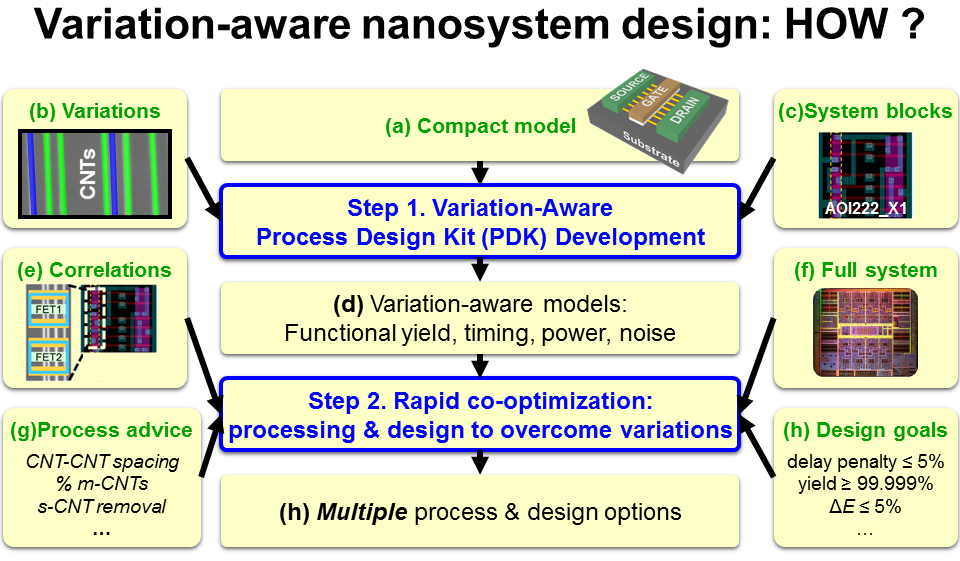
The NDK design flow consists of two steps (illustrated using CNFETs, though other technologies and compact models may be used as well), described as follows (and shown in the figure below):
-
Variation-aware Process Design Kit (PDK) development – statistical models of (CNFET) variability that are relevant from a system perspective, and characterization/modeling procedures for such variations, with validation using experimental data. This approach is illustrated for standard library cells.
-
Rapid co-optimization of processing and circuit design to overcome (CNT) variations – (CNFET) design methodologies addressing variability (including integrated approaches for statistical timing, power analysis, yield and noise analysis). The approach is illustrated for large design blocks such those from the OpenSparc T2 SoC.
Download
The NDK is available for download as a single bundle here: https://nanohub.org/resources/22582. It includes a detailed user guide describing how to setup the environment, install all required packages, and run the NDK. Example scripts for creating variation-aware timing, power, and noise models for CNFET-based standard library cells, and for using these models to design modules from the processor core of OpenSparc T2 using CNFETs, are also provided.
NDK intended to be executed in a unix environment. It relies on the following external tools (which the user should have access to).
|
Tool
|
Purpose
|
|---|---|
|
hspice
|
Circuit simulations using compact models
|
|
MATLAB
|
Calibrating variation-aware timing, power, and noise models
|
|
Perl
|
Automatic script generation
|
|
Synopsys design compiler
|
Synthesis
|
|
Cadence encounter, Synopsys IC compiler, Capo (UMich PD tools, see below)
|
Place & route
|
|
gcc
|
C++ compiler
|
Additionally, the user should download the following external packages, which are also required by the NDK.
|
Package
|
Description
|
|---|---|
|
CNFET compact device model, as described by the following papers:
|
|
|
Standard cell library views for the 15 nm technology node, required for variation-aware timing, power, and noise models for standard cells
|
|
|
Convex Optimization packages, required for calibrating variation-aware timing, power, and noise models
|
|
|
Full system description of the OpenSparc T2 processor, includes verilog
|
|
|
Various physical design tools, required for circuit-level analysis
|
|
|
Various C++ helper functions, required for circuit-level analysis
|
|
|
Performing matrix operations, required for circuit-level timing, power, and noise margin analysis
|
|
|
Numerically solving multi-variate normal cumulative distribution functions, required for circuit-level noise margin analysis
|
Documentation
The following papers demonstrate how to overcome CNT variations through co-optimized processing and circuit design, using the NDK:
- G. Hills, J. Zhang, C. Mackin, M. M. Shulaker, H. Wei, H.-S. P. Wong, and S. Mitra. "Rapid Exploration of Processing and Design Guidelines to Overcome Carbon Nanotube Variations,” Proceedings of the 50th Annual Design Automation Conference, p. 105. ACM, 2013.
- G. Hills, J. Zhang, M. M. Shulaker, H. Wei, C.-S. Lee, A. Balasingam, H.-S. P. Wong, and S. Mitra, “Rapid Co-optimization of Processing and Circuit Design to Overcome Carbon Nanotube Variations,” IEEE Transactions on Computer-Aided Design of Integrated Circuits and Systems, vol. 34.7, pp. 1082-1095, 2015. (Additional details describing the design flow are available in the Appendix).
Additional references published by our group can be found here.
Discussion Forum
Any comments, suggestions, new module/enhancement requests, and bug reports maybe be filed in the discussion forum.