You must login before you can run this tool.
PN Junction Lab (New Interactive Front End)
Visualize and explore P-N junction concepts fully interactively: Band Edge Diagrams, Charge Densities, I-V and C-V Characteristics
Newer version available


Category
Published on
Abstract
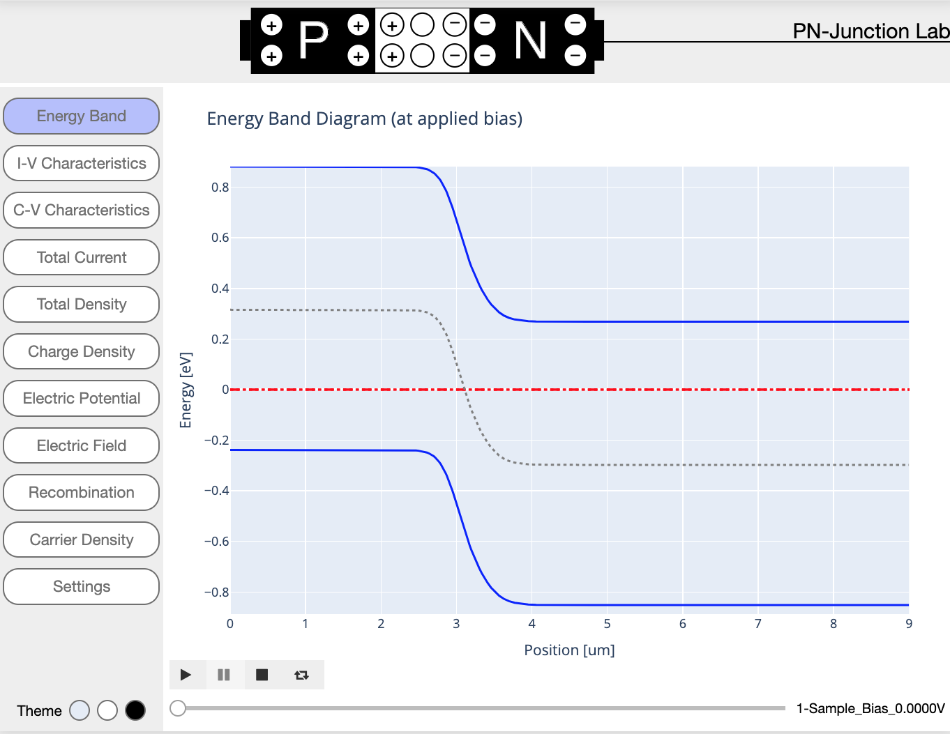
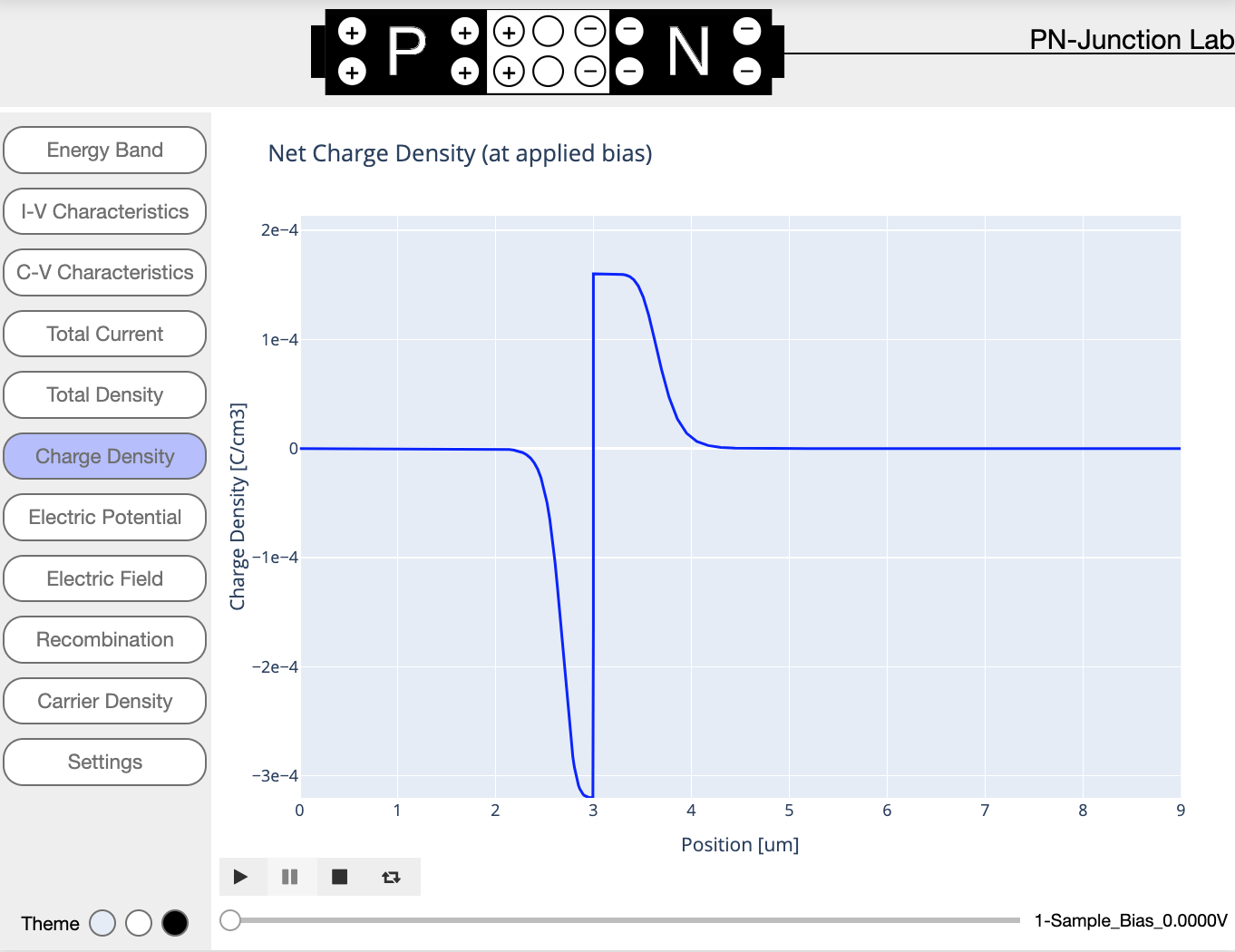
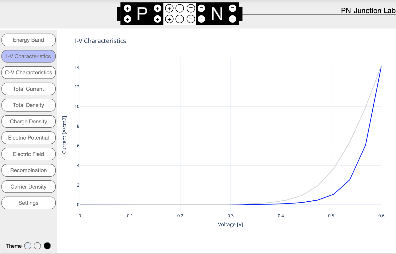
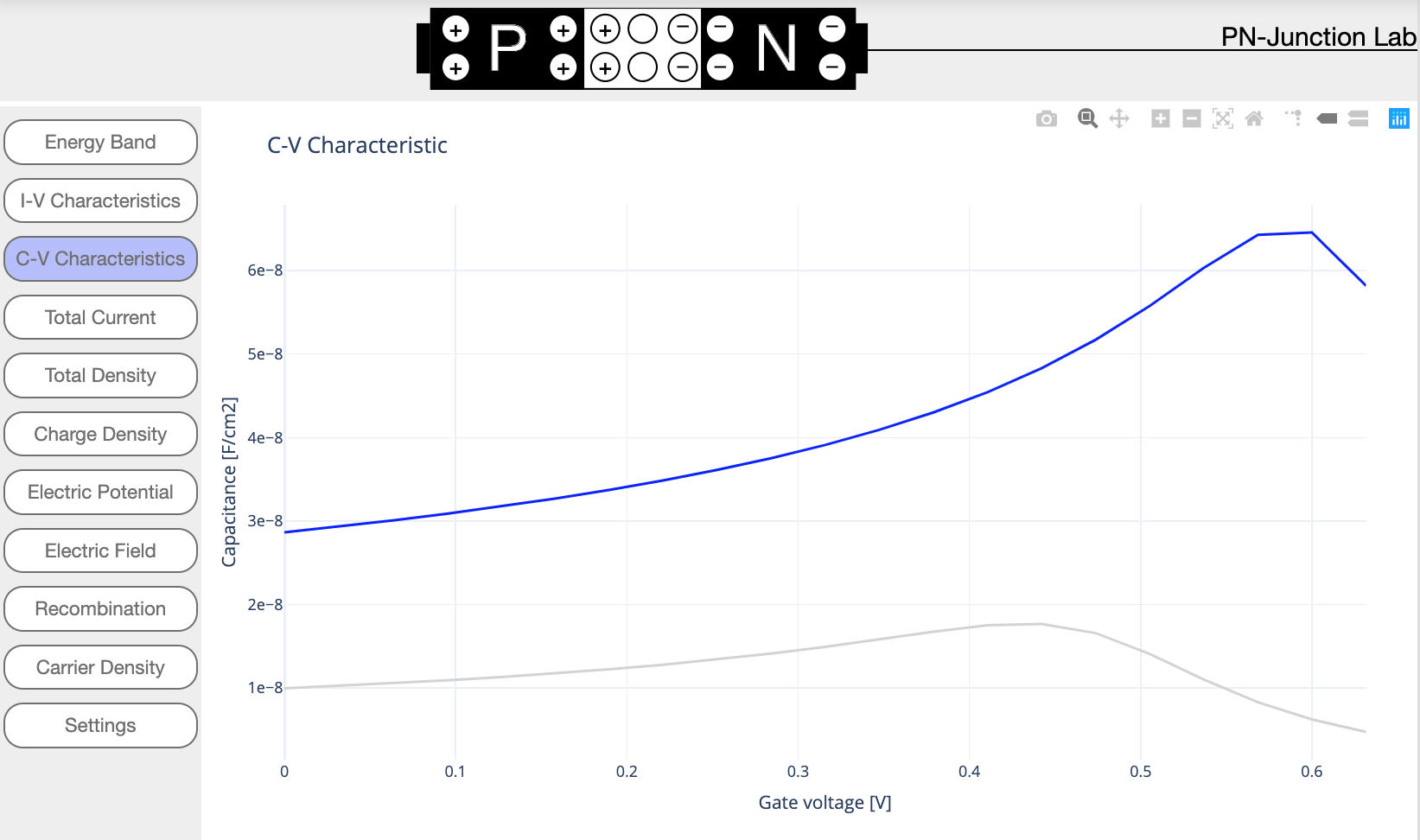
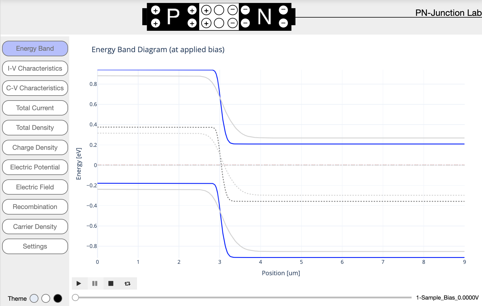
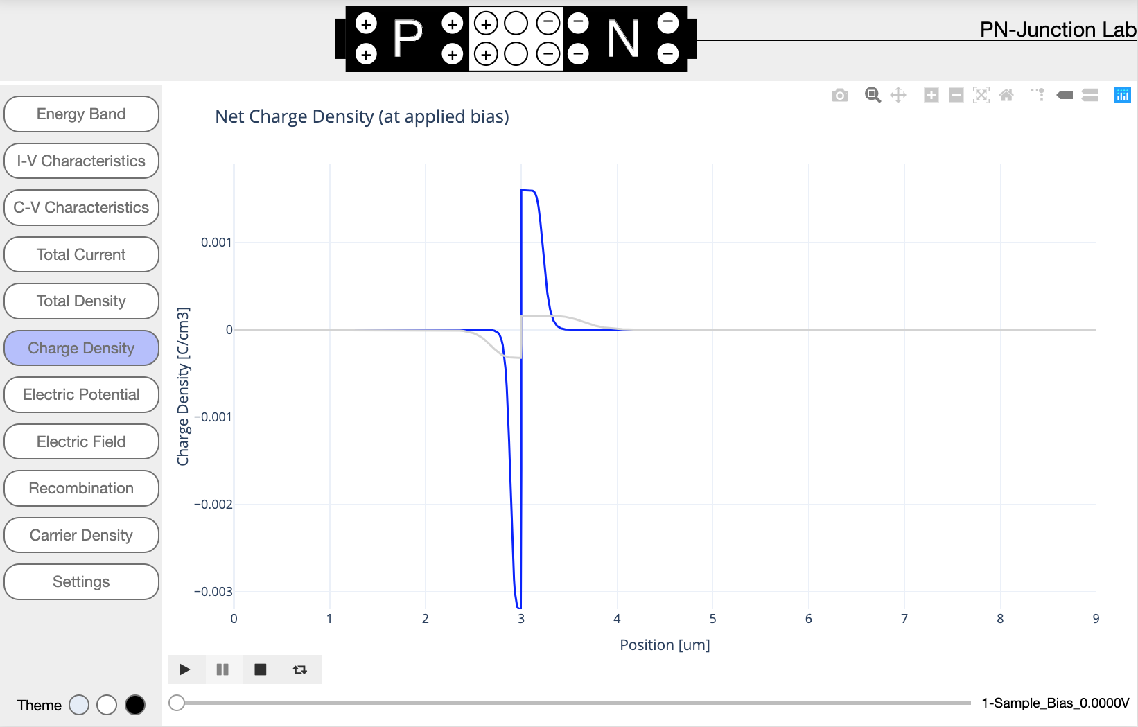
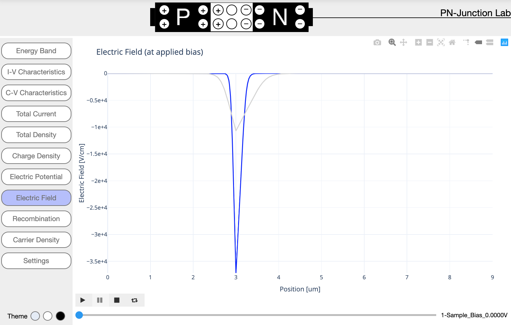
PN Junction Lab - is a fully interactive app that enables the visualization and exploration of P-N junctions. Users immediately see the conduction and valence band diagrams as well as the quasi-Fermi levels as the app starts up. A slider at the bottom enables users to pan through various bias points and visualize the band-edge diagram as a function bias. Other critical quantities such as charge densities, electric fields, current densities as well as full current-voltage and capacitance-voltage characteristics can be explored interactively with a click of a button.
New simulations can be launched to explore different doping concentrations and temperatures. Different materials such as Si, Ge, GaAs, and InP are available for exploration.
Different PN-junction geometries such as short p or n regions which bring the surface recombination closer to the junction. Advanced users can explore the effects different minority carrier lifetimes.
The simulations are performed with a full industrial strength device simulation tool. Numerical issues such as number of numerical nodes included in the simulation (i.e. meshing) can also be explored.
This new PN Junction Lab is powered by the previous Rappture-Based PN-Junction Lab but provides a much more interactive user experience. The industrial strength PADRE tool developed at Bell Labs ultimately powers the simulations.
Cite this work
Researchers should cite this work as follows: