You must login before you can run this tool.
Crystal Viewer Tool
Visualize different crystal lattices and planes
Version 3.0.9 - published on 29 Jan 2020
doi:10.21981/K3EK-R382 cite this
This tool is closed source.
Newer version available


Category
Published on
Abstract
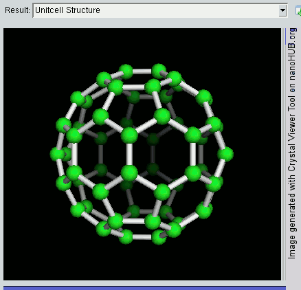
Crystal Viewer 3.0 is a new tool starting from scratch. It is designed based on the old version 2.3.4 and aims to include better visualization and new features. It visualizes 14 Bravais lattices, Miller planes, and crystal structures of specific materials needed for many courses in materials, electronics and chemistry. Users can also create and view materials not contained in our database by setting certain material properties like the basis atom position, the Bravais vector. The main purpose of this educational tool is to provide insight about the crystalline structure of various materials.
For problems with this tool, please submit a support ticket (click on "Need Help?" button in upper right part of this page). To submit a wish for improvements, please click on the Wishlist tab above.
First Time User Guide: This document provides useful information to the users who are using the tool for the first time. It explains some important details about crystallography and usage of the tool..
Version History:
Version 3.0 (Oct 2014)
- Initial publish
Version 3.0.2 (Jan 2015)
- Add "text book" unit cell plotting for all cubic system materials
Version 3.0.3 (May 2016)
- Add several materials: Bi2Te3, SrTiO3, MoS2, Black Phosphorous
- Add Graphene AB stacking
Wish List:
- See this link for an elaborate wishlist of the tool.
Powered by
NEMO 5, a code under development in the research group of Gerhard Klimeck. NEMO 5 is an open source nanoelectronics device simulator containing a variety of different material and geometry models. Features include the construction of atomistic grids of varying crystal structures, multiband Schroedinger-Poisson simulations, atomistic strain and phonon computations, quantum transport using open-boundary wavefunctions or NEGF, and user-friendly input/output.
Credits
Crystal Viewer 3.0 was written and developed by Yuanchen Chu as a PhD student at Purdue University.
Various people are also involved in the development of Crystal Viewer 3.0:
Travis Shepherd, Yosef Borga, Vincent Ntarugera, Kevin Margatan, Zach Shaffter... SURF program students summer intern (< V3.0)
G. Klimeck, H.-H. Park, J. Fonseca, J. Sellier, M. Povolotskyi, S. Steiger, T. Kubis... NEMO 5 simulation engine (in alphabetical order)
Fan C... Add Graphene AB Stacking Visualization and SrTiO3
Tanya... Feature and design suggestion
The main author Yuanchen Chu is obliged to D. Mejia, G. Klimeck, J. Fonseca, M. Povoltskyi, T. Faltens for the valuable information and advice provided by them.
Sponsored by
Network for Computational Nanotechnology (NCN), Purdue University
References
Robert F. Pierret, Purdue University, Advanced Semiconductor Fundamentals (Second Edition).
ISBN-10: 013061792X • ISBN-13: 9780130617927 ©2003 • Prentice Hall
Cite this work
Researchers should cite this work as follows: