IWCN 2021: Interfacial Trap Effects in InAs Gate-all-around Nanowire Tunnel Field- Effect Transistors: First-Principles-Based Approach
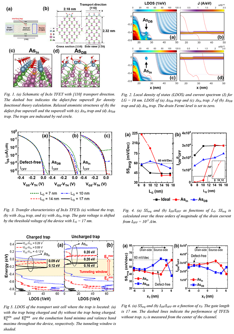
Interfacial Trap Effects in InAs Gate-all-around Nanowire Tunnel Field- Effect Transistors: First-Principles-Based Approach
-
 1. Interfacial Trap Effects in In…
0
00:00/00:00
1. Interfacial Trap Effects in In…
0
00:00/00:00 -
 2. Outline of Presentation
20.02002002002002
00:00/00:00
2. Outline of Presentation
20.02002002002002
00:00/00:00 -
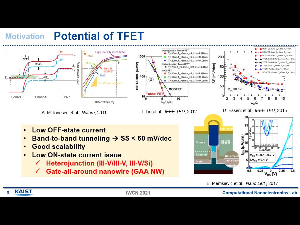 3. Potential of TFET
45.879212545879213
00:00/00:00
3. Potential of TFET
45.879212545879213
00:00/00:00 -
 4. Defect-induced degradation
95.061728395061735
00:00/00:00
4. Defect-induced degradation
95.061728395061735
00:00/00:00 -
 5. Defect models – previous wor…
168.6353019686353
00:00/00:00
5. Defect models – previous wor…
168.6353019686353
00:00/00:00 -
 6. Contribution
269.06906906906909
00:00/00:00
6. Contribution
269.06906906906909
00:00/00:00 -
 7. Outline of Presentation
296.26292959626295
00:00/00:00
7. Outline of Presentation
296.26292959626295
00:00/00:00 -
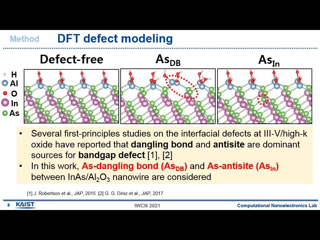 8. DFT defect modeling
307.2072072072072
00:00/00:00
8. DFT defect modeling
307.2072072072072
00:00/00:00 -
 9. DFT defect modeling
338.53853853853855
00:00/00:00
9. DFT defect modeling
338.53853853853855
00:00/00:00 -
 10. DFT defect modeling
388.02135468802135
00:00/00:00
10. DFT defect modeling
388.02135468802135
00:00/00:00 -
 11. Mode-space in heterostructures
449.61628294961628
00:00/00:00
11. Mode-space in heterostructures
449.61628294961628
00:00/00:00 -
 12. NEGF Phonon scattering
473.47347347347352
00:00/00:00
12. NEGF Phonon scattering
473.47347347347352
00:00/00:00 -
 13. Simulation setup / parameters
533.06639973306642
00:00/00:00
13. Simulation setup / parameters
533.06639973306642
00:00/00:00 -
 14. Outline of Presentation
551.0510510510511
00:00/00:00
14. Outline of Presentation
551.0510510510511
00:00/00:00 -
 15. Supercell band structures
555.88922255588921
00:00/00:00
15. Supercell band structures
555.88922255588921
00:00/00:00 -
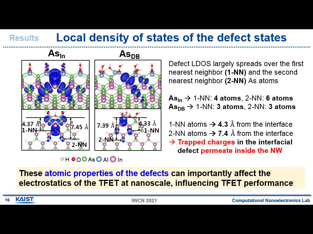 16. Local density of states of the…
604.07073740407077
00:00/00:00
16. Local density of states of the…
604.07073740407077
00:00/00:00 -
 17. Energy-resolved DOS (NEGF)
670.67067067067069
00:00/00:00
17. Energy-resolved DOS (NEGF)
670.67067067067069
00:00/00:00 -
 18. Density-averaged potential
708.34167500834167
00:00/00:00
18. Density-averaged potential
708.34167500834167
00:00/00:00 -
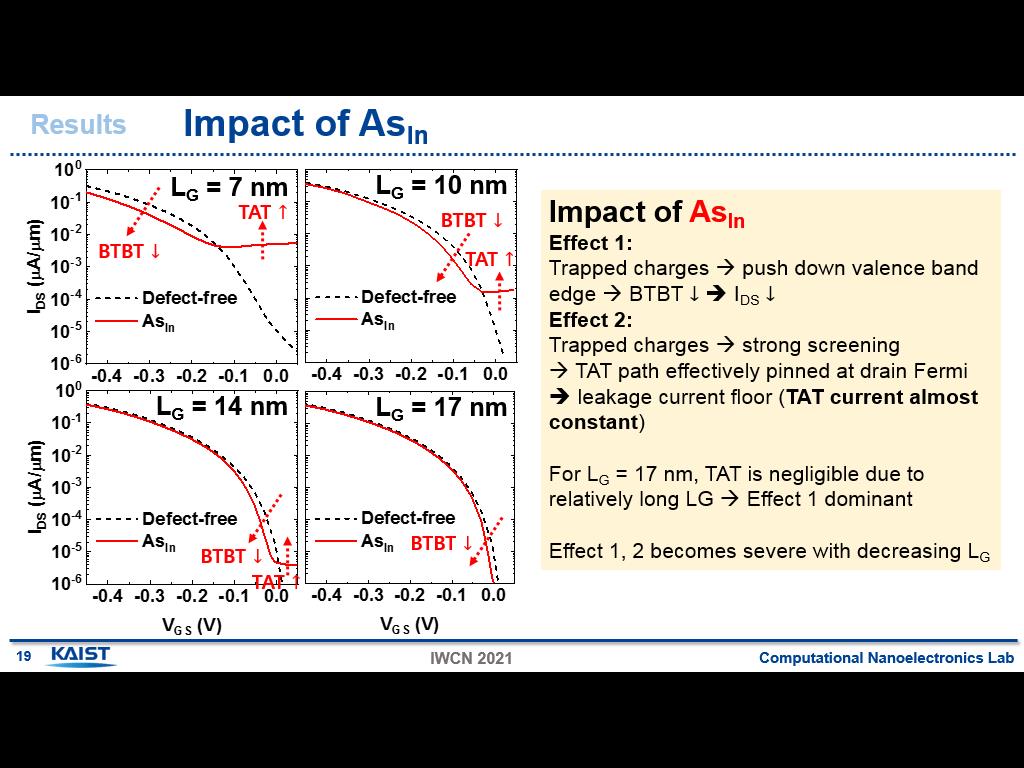 19. Impact of AsIn
749.88321654988329
00:00/00:00
19. Impact of AsIn
749.88321654988329
00:00/00:00 -
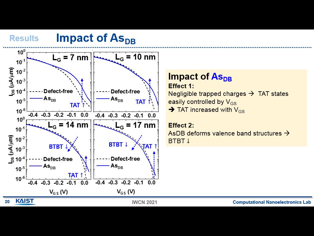 20. Impact of AsDB
803.53687020353686
00:00/00:00
20. Impact of AsDB
803.53687020353686
00:00/00:00 -
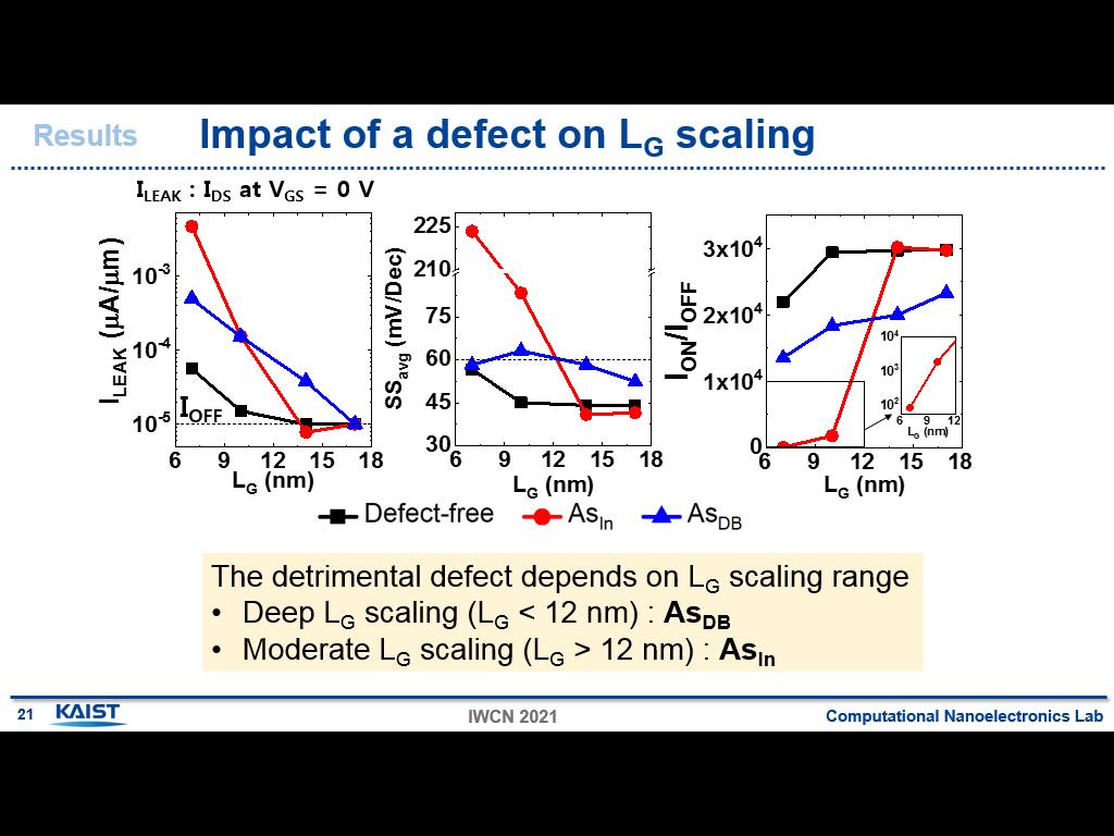 21. Impact of a defect on LG scali…
836.56990323657
00:00/00:00
21. Impact of a defect on LG scali…
836.56990323657
00:00/00:00 -
 22. Outline of Presentation
866.16616616616625
00:00/00:00
22. Outline of Presentation
866.16616616616625
00:00/00:00 -
 23. Conclusions
870.93760427093764
00:00/00:00
23. Conclusions
870.93760427093764
00:00/00:00