You must login before you can run this tool.
Band Structure Lab
Computes the electronic and phonon structure of various materials in the spatial configuration of bulk , quantum wells, and wires
Version 3.1.14 - published on 16 Sep 2022
doi:10.21981/C9QG-4893 cite this
This tool is closed source.
Category
Published on
Abstract
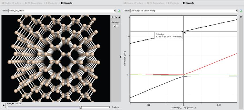
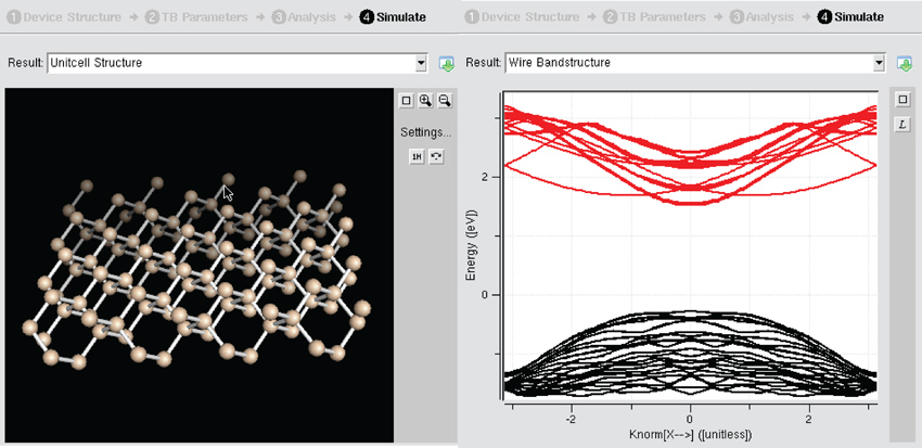
Band structure Lab uses the sp3s*d5 tight binding method to compute E(k) for bulk, planar, and nanowire semiconductors. Using this tool, you can quickly compute and visualize the band structures of bulk semiconductors, thin films, and nanowires for various materials, growth orientations, and strain conditions. Physical parameters such as the bandgap and effective mass can also be obtained from the computed E(k). The bandedges and effective masses of the bulk materials and the nanostructures structures can be analyzed as a function of various strain conditions.
As explained in a related seminar, correct band structure is essential for modeling devices at the nano scale.
- Chapter 5 of Quantum Transport by S. Datta (Cambridge, 2005)
Band Structure Lab is powered by NEMO5. Previous versions were powered by OMEN and Matlab. We very much appreciate feedback if certain features of the tool do not function properly. The previous 2.x version of Band structure Lab is still available under the "versions" tab.
Click here to learn more about NEMO5
Physical Limitations:
- Different Tight-binding models can give different electron and hole effective masses. This happens since different band models give different curvatures.Always a higher and more sophisticated band model will give better estimation of effective masses. Eg: sp3d5s* TB models give better estimate of effective mass compared to sp3s* TB models.
Tool Versions
- 2.0.1: Bug Fixes :
- Strain sweep now provides correct band edges as well as effective mass values for bulk
- 2.0.1 New Features: Following new features will be available in the next release of the tool:
- Transport effective masses for nanowires and UTB devices.
- Self-consistent run for nanowire Gate all around FETs and DGMOS
- 2.0.2 Bugfixes:
- Bulk effective masses for light, and heavy hole bands have been corrected.
- Charge self-consistent simulations are now stable.
- Biaxial strain sweep related error has been removed. Now all the results appear that have completed.(Answer to the biaxial question too.
- 2.0.2 New Features :
- Transport effective masses for nanowires and UTB devices are now available.
- Now 3D EK simulation data available with 3D bulk simulation as data file. (Answer to this question .
- Self-consistent run for 1 gate bias now possible for Gate all around nanowire FETs and DGMOS
- 2.0.3 New Features
- Parallel execution on 24 cores in an instant-on parallel computing environment where appropriate. Used for nanowires and ultra-thin bodies with not too large cross section.
- Fixed the tool tip for wires and utb making them more appropriate and correct. Fixed the problem pointed in this question
2.0.7 Bug-Fixes:
- Some minor corrections done to the job submission script
- 2.0.8 Bug-Fixes:
- Fixed the 3D Bulk BZ representation. Now the simulation works on all clusters. Granted this wish
- Fixed the bulk EK for InAs and obtain the correct effective masses.
- Fixed the strain sweep for the Bulk materials. Also the discrepancy with the strain labels have been fixed which answers the question1 and question 2
- Hydrostatic strain in InAs has been corrected.
2.0.8 Improvements: - New strain model has been implemented in the code. This also answers this question .
- Uniaxial strain [110] has been corrected for Bulk Silicon.
2.0.9 Bug-Fixes: - Fixed the Strain calculation which broke in the last revision. This solves the problem recently reported here
- UTB Ek for X2 direction corrected and also the fullband simulation corrected.
2.0.9 Improvements: - The Abort button has been implemented in the tool now after some changes to the method of job launching and submission. This also answers this question .
- Status messages while jobs are running have been changed and improved. Allows the users to get more up to date status of their jobs.
3.0.0 Improvements: - Tool migrated to a new underlying simulation engine NEMO5 from OMEN. This has enhanced computational capabilites and can compute bandstructures of different wires and new geometries like Core-Shell. Can also perform self consistent E-k calculations for ultra thin bodies and wires. The last 2.0.15 version of Band structure Lab powered by OMEN is still available at the following link: Bandstructure Lab Version 2.0.15
3.0.5 Improvements: - Effective mass calculation added.
3.1.0 Improvements: - Phonon bandstructure calculation has been introduced
- Alloy materials have been included with unfolding features. Collaboration: Simulation of larger structures and new materials can be done on collaborative basis. We would like to know what you want to achieve and we can work towards it. Please feel free to contact the developers of the tool.
- 3.1.8 Improvements:
- Add Keating valence force field (VFF) model and modified VFF model that includes 3rd nearest neighbor for silicon.
- Add Keating VFF model and enhanced VFF model for the lattice properties of GaAs.
- Fix the bug of the phonon dispersion calculation for the alloy structure with random alloy and virtual crystal approximation (VCA).
- Implement the phonon dispersion calculation within UTB structure and nanowire.
- 3.1.13 Improvements:
- Code fails on triangular wires. Eliminated the option for now
- Extended time range for some the code to run to complete larger cross section simulations.
- Added "CentralBands" to the output option in Bulk to focus on the relevant valence and conduction bands.
- Utilize NEMO release 17881 to ensure the strain calculations in wires and utb work again.
- Added structure output to the phonon calculations
- Changed the "Bands" label which was shared in Bulk, Wire, and UTB calculations to distinct labels since the k-grid and energy range is quite different anyhow and the graphical overlap is not really possible at this stage.
- 3.1.14 Improvements:
- Reduce the number of default sweep points in bulk strain calculations from 11 to 3 to speed up the calculations. Users can increase the number as needed.
Powered by
NEMO5
Credits
Bandstructure Lab is based on the tight binding model of Boykin and Klimeck, and builds on the work of several Ph.D. students and other researchers:
K. Miao... Add different phonon models, begining with Version 3.1.8. S. Mukherjee... Introduced phonons, random alloys beginning ver 3.1.0 S. Mukherjee... Migration to NEMO5 beginning ver 3.0.0 M. Luisier, A. Paul... Core C simulator, beginning with Version 2.0A. Paul, J. Geng... GUI development and OMEN integration of version 2.0, Code Matainance and improvementsM. Luisier, N. Neophytou, Y. Liu... Core Matlab simulator, prior to Version 2.0 A. Matsudaira, M. McLennan... GUI development of version 1.0R. Kim... Led the integration effort of Version 1.0J. Wang, N. Neophytou... Nanowire simulation theoryA. Rahman... Bulk and thin-film simulation theory
Sponsored by
NCN@Purdue, MSD FCRP, SRC
Cite this work
Researchers should cite this work as follows:
-
- For the tight-binding methodology: Gerhard Klimeck, Fabiano Oyafuso, Timothy B. Boykin, R. Chris Bowen, and Paul von Allmen, "Development of a Nanoelectronic 3-D (NEMO 3-D) Simulator for Multimillion Atom Simulations and Its Application to Alloyed Quantum Dots" (INVITED), Computer Modeling in Engineering and Science (CMES) Volume 3, No. 5 pp 601-642 (2002).
- For nanowire model and results: Jing Wang, Anisur Rahman, Gerhard Klimeck and Mark Lundstrom, "Bandstructure and Orientation Effects in Ballistic Si and Ge Nanowire FETs", IEEE International Electron Devices Meeting (IEDM) Tech. Digest, pp. 537-540, Washington D. C., Dec. 5-7, 2005.
-
Samik Mukherjee, Kai Miao, Abhijeet Paul, Neophytos Neophytou, Raseong Kim, Junzhe Geng, Michael Povolotskyi, Tillmann Christoph Kubis, Arvind Ajoy, Bozidar Novakovic, James Fonseca, Hesameddin Ilatikhameneh, Sebastian Steiger, Michael McLennan, Mark Lundstrom, Gerhard Klimeck (2022), "Band Structure Lab," https://nanohub.org/resources/bandstrlab. (DOI: 10.21981/C9QG-4893).